MA1916
1/11
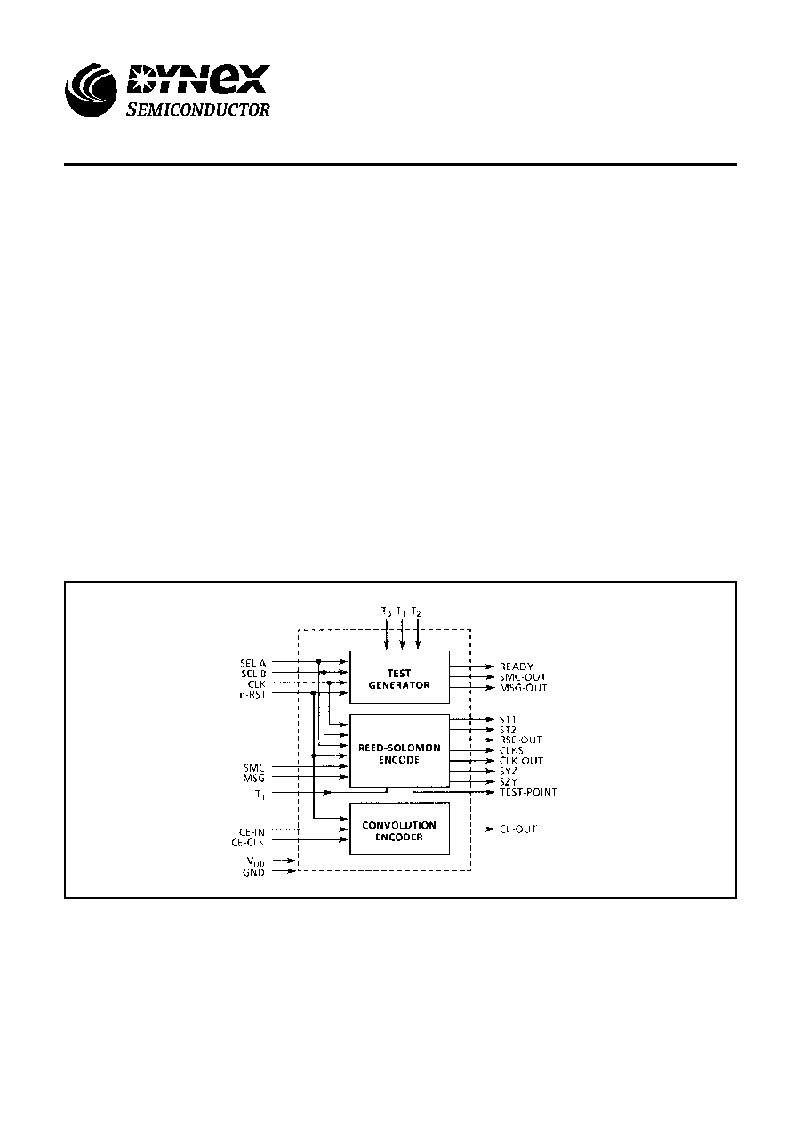
The purpose of the MA1916 is to encode serial data to
allow error correction when the data is transmitted over a noisy
communication link. As the name suggests, the unit contains
two encoding elements. The Reed-Solomon encoder appends
a checksum to a block of data, guarding against burst errors in
a message. The convolution encoder continuously creates two
code bits for each data bit it receives, increasing the noise
immunity by doubling the band width of the message. The unit
also contains a test pattern generator which can be connected
to check the functionality of the RS encoder and to provide a
message timing signal (SMC_OUT).
Protection against a long error-burst can be increased by
interleaving a number of message packets passing through
the RS encoder. The MA1916 provides pin selectable
interleave depths of 1, 4 or 5. Interleave depths of greater than
5 do not significantly improve performance.
The MA1916 is designed to conform to the CCSDS
standard for telemetry 101.0.B.2. It is manufactured in a
radiation hard low power CMOS technology. This makes it
ideal for use in satellite communications systems. The encoder
reduces the risk of data corruption and allows the designer to
minimize the transmitter power needed to establish an
effective communications link.
FEATURES
s
Radiation Hard CMOS-SOS Technology
s
Low Power Consumption
s
Latch-up Free
s
High SEU Immunity
s
CCSDS Standard RS (255, 223)
s
Selectable Interleave Depths of 1, 4 or 5
s
5MBit/sec Input Data Rate
Figure 1: Block Diagram
MA1916
Radiation Hard Reed-Solomon
& Convolution Encoder
Replaces June 1999 version, DS3590-4.0
DS3590-5.0 January 2000

MA1916
2/11
OPERATION
REED-SOLOMON ENCODER
The function of the Reed-Solomon (RS) encoder is to take
a block of 223 bytes of serial data and to append a checksum
of 32 bytes. The purpose of the checksum is to allow error
correction within the data block. One important feature of the
Reed-Solomon algorithm is that it allows correction of a burst
error which corrupts upto 16 consecutive bytes. If a number of
messages are interleaved this length can be increased. The
MA1916 provides pin selectable interleave depths of 1, 4 or 5
blocks (see Table 1), each of 223 bytes. An interleave depth of
5 is the maximum recommended by the CCSDS standard.
This will allow correction of up to 80 sequencial bytes in a data
packet.
The RS encoder operates from a clock input CLK which
must be driven at twice the input data rate. Internally CLK is
divided to give a clock CLKS which runs at half the frequency.
This signal is available as an output and is used to time data
into the RS encoder.
A high input on SMC is used to tell the RS encoder that
data to be encoded is present on the MSG pin (see Figure 2).
While SMC is high the data on MSG is buffered and appears
on RSE_OUT as well as being clocked into the encoder. As
soon as SMC goes low the checksum is clocked out of the
encoder onto RSE_OUT.
While SMC is high the RSE_OUT signal follows the input
MSG. When SMC is low RSE_OUT is produced from the
exclusive-OR of MSG and the checksum signal. For this
reason MSG must be held low while the encoder outputs the
checksum.
A gap can be left between successive data packets by
holding SMC and MSG low after the checksum has been sent.
Alternatively, synchronisation code can be inserted before a
data block by holding SMC low and placing the code on MSG.
As soon as SMC goes high any further data on MSG is
assumed to form part of a message and will be encoded
accordingly.
Note: External logic must guarantee the SMC is high for
the correct period, ie only while 223 x I bytes (I = interleave
depth) of data are clocked through. Otherwise when SMC falls
an invalid checksum will be produced.
SEL_A
SEL_B
Interleave
SMC_OUT Period (Bytes)
I = Depth
SMC_OUT = 1 SMC_OUT = 0
0
0
5
5 x 223
5 x 32
0
1
4
4 x 223
4 x 32
1
0
1
1 x 223
1 x 32
1
1
5
5 x 223
5 x 32
I = Interleave depths of 1, 4 or 5
SYNC:
If SMC is low and no checksum is being output any data on MSG will appear on RSE_OUT.
This feature can be used to insert a synchronisation sequence before a data block.
DATA:
Data block 223 x I bytes in length.
CHECKSUM:
The checksum is 32 x I bytes long and appended to the data by the RS encoder.
Figure 2: Reed-Solomon Encoder Operation
Table 1: Interleave Length Defined by SEL_A and SEL_B
MA1916
3/11
CONVOLUTION ENCODER
The convolution encoder generates 2 serial bits of output
data for each bit it reads in. The coding operates cyclically over
a length of 7 bits. It increases the bandwidth of the signal but
establishes a correlation between succesive bits in the output
signal.
The convolution encoder operates continuously using
CE_CLK to read data in on CE_IN and to write the encoded
data to CE_OUT.
If required the output of the Reed-Solomon encoder can be
fed directly into the convolution encoder by connecting
RSE_OUT to CE_ IN and CLKS to CE_CLK.
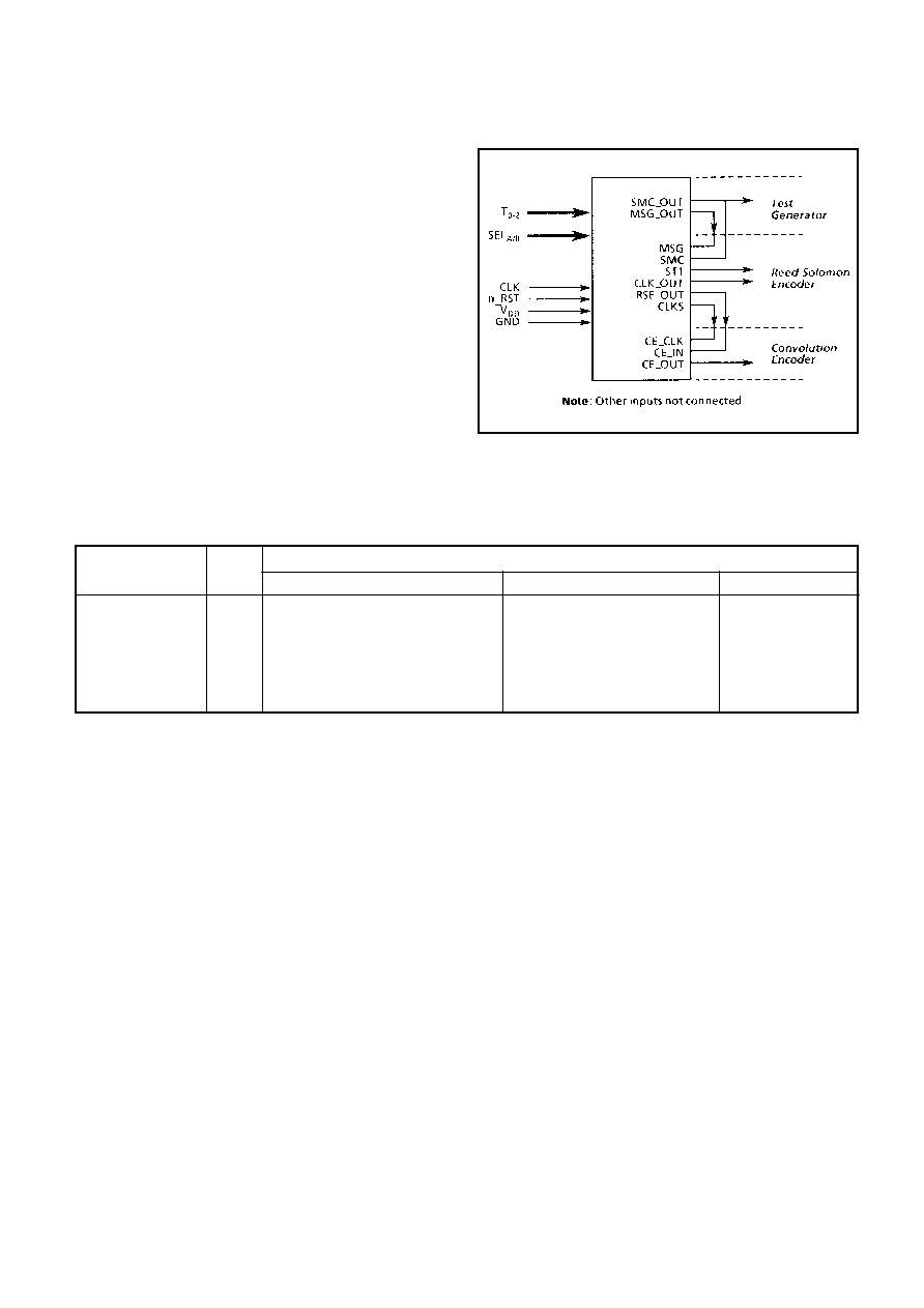
TEST GENERATOR
The MA1916 contains its own built-in test pattern
generator, this can be connected to the RS encoder for in
service testing. The test generator supplies test patterns and
the SMC signal according to the inputs on T0-2 (see Table 2)
and the interleave depth selected using SEL_A and SEL_B.
Figure 3 shows the necessary connections for feeding test
patterns through both the RS and the convolution encoder.
Figure 3: Test Configuration
Table 2: Test Pattern on MSG_OUT Defined by T0-2
PIN DESCRIPTION
V
DD
and GND (Power and Ground)
The MA1916 uses a single power supply of 5V
�
10%.
CLK (Clock)
This input supplies a clock signal to the RS encoder and
the Test generator. It requires a signal with a nominal 50%
duty cycle running at twice the input data rate for the RS
encoder. The rising edge of CLK is used to generate the
internal CLKS signal which clocks data through the RS
encoder.
n_RST (Reset)
This active low signal is a reset supplied to the RS encoder,
the test generator and the convolution encoder. It should be
noted that the reset does not clear the check sum in the RS
encoder and a complete dummy data packet should be run
through before valid data is sent.
SEL_A and SEL_B (Interleave Depth Select)
These inputs define the interleave depth of a message
passing through the RS encoder They also specify the
message length to be produced by the test generator (see
Table 1). The inputs are connected to internal pulldown
resistors.
T
0-2
(Test Pattern Select)
These inputs select the pattern to be produced by the test
generator (see Table 2). Each input is connected to an internal
pull-down resistor.
T
3
(Production Test Input)
This input is used for production testing only It has an
internal pull-down resistor and should be left unconnected .
MSG_OUT (Test Message Output)
This output pin carries the test patterns defined by the
inputs To-2 and produced by the test generator. This signal
can be connected directly to MSG for testing purposes.
Interleave Depth
T2
T1
T0
Test
I = 5 (1115 bytes)
I = 4 (892 bytes)
I = 1 (223 bytes)
0
0
0
N/A
0
0
0
1
1
(1, 2, 3, 4, 5) x 223
(1, 2, 3, 4) x 223
(1) x 223
0
1
0
2
(0) x 222 x 5, (0) x 4, (7B)
(0) x 222 x 4, (0) x 3, (7B)
(0) x 222, 7B
0
1
1
3
(0) x 222 x 5, (7B, AF, 99, FA, B7)
(0) x 222 x4, (7B, AF, 99, FA)
(0) x 222, 7B
1
0
0
4
(0) x 221 x 5, (7B) x 5, (47) x 5
(0) x 221 x 4, (7B) x 4, (47) x 4
(0) x 222, 7B
Other
N/A

MA1916
4/11
SMC_OUT (Select Message or Checksum)
This output signal is held high while the test generator clocks
out a data packet on the MSG_OUT pin. When the packet is
complete this signal goes low. It is held low for a period equal to
the time required by the RS encoder to send the corresponding
checksum. When this is complete the signal goes high and the
test generator begins a new data packet. This signal can be
connected directly to SMC for testing purposes.
READY (Test Data Valid)
This output is held low during reset and remains low for the
first complete cycle of SMC_OUT. READY rises on the second
rising edge of SMC_OUT and remains high to indicate the
presence of valid data on MSG_OUT.
CLKS (Synchronisation Clock)
This output clock runs at half the speed of the input clock
CLK. CLKS remains low after n_RST is raised until SMC is
raised, SMC being captured on the falling edge of CLK (timing
4). CLKS then changes state on the rising edge of each CLK
cycle regardless of the state of SMC. The signal is used to
clock data into and out of the RS encoder.
MSG (Message)
MSG is the data input to the RS encoder. Each bit is read in
on the rising edge of CLKS. While the SMC signal is high data
on the input passes directly to the output RSE_OUT. While
SMC is low RSE_OUT is the logical XOR of the MSG input and
the output of the check-sum generator. Therefore MSG must
be held low while the RS encoder is clocking out the check
sum (see Figure 4).
SMC (Select Message or Checksum)
While the SMC input is high, data on the MSG pin is
clocked into the RS encoder. SMC is held high for a period
dictated by the interleave depth being used (see Table 1).
When SMC falls the RS encoder begins to clock out the
checksum for the preceeding data. SMC should be held low
until the complete checksum has been output. The rising edge
of SMC indicates the start of a new data block to be encoded.
RSE_OUT (Reed-Solomon Encoder Output)
This signal outputs the completed data packet comprised
of the message followed by its associated checksum block.
The data is valid on the rising edge of CLKS.
Figure 4: Reed-Solomon Encoder
ST1 (RS Encoder Output Valid)
This output is set low during a reset and goes high when
sufficient dummy data has been clocked through the RS
encoder to clear it (see Figure 5).
SYZ (Byte Rate Clock)
SYZ is a byte rate clock output derived from CLKS. It is
high during every eighth period of CLKS and low at other
times.
SZY (Byte Rate Clock)
SZY is a byte rate clock output derived from CLKS. It is low
during every eighth period of CLKS and high at other times. It
is the inverse of SYZ.
ST2 (Production Test Output)
The output is used for production testing and should be left
unconnected.
TEST_POINT (Production Test Output)
This output is used for production testing and should be left
unconnected.
CE_IN (Convolution Encoder Data In)
This input is used to read data into the convolution
encoder. The state of CE_IN is read on the rising edge of
CE_CLK.
Figure 5: Reed-Solomon Encoder Operation
SMC
MSG
CLKS
ST1
n_RST
Output Valid
Note: ST1 rises on the second rising edge of SMC following n_RST high.
CLKS starts toggling on the first rising edge of SMC following n_RST high.
MA1916
5/11
DC CHARACTERISTICS AND RATINGS
Parameter
Min
Max
Units
Supply Voltage
-0.5
7
V
Input Voltage
-0.3
V
DD
+0.3
V
Current Through Any Pin
-20
+20
mA
Operating Temperature
-55
125
�
C
Storage Temperature
-65
150
�
C
CE_CLK (Convolution Encoder Clock)
The CE_CLK input drives the timing of the convolution
encoder. Data is read in on CE_IN on the rising edge of
CE_CLK and output on CE_OUT on both the rising and falling
edge of CE_CLK.
Note: The output data rate is twice the input data rate.
A 50% duty cycle clock is required. If this is provided by the
CLKS output, data can be read directly from RSE_OUT to the
CE_IN input (see figure 3).
CE_OUT (Convolution Encoder Output)
This signal carries the output data from the convolution
encoder. The data rate on CE_OUT is twice that of CE_IN.
CLK_OUT (Clock Out)
CLK_OUT is a buffered output of the CLK input signal. If
CLKS is connected to CE_CLK to drive the convolution
encoder, CE_OUT can be captured on the falling edge of
CLK_OUT.
Note: Stresses above those listed may cause permanent
damage to the device. This is a stress rating only and
functional operation of the device at these conditions, or at
any other condition above those indicated in the operations
section of this specification, is not implied. Exposure to
absolute maximum rating conditions for extended periods
may affect device reliability.
Table 3: Absolute Maximum Ratings
Symbol
Parameter
Conditions
Min
Typ
Max
Units
V
DD
Supply Voltage
-
4.5
5.0
5.5
V
V
IH
CMOS Input High Voltage
V
DD
= 5.5V
0.8 V
DD
-
V
DD
V
V
IL
CMOS Input Low Voltage
V
DD
= 5.5V
V
SS
-
0.2 V
DD
V
V
OH
CMOS Output High Voltage
V
DD
= 5V, I
OH
= -1.0mA
V
DD
-0.5
-
-
V
V
OL
CMOS Output Low Voltage
V
DD
= 5V, I
OL
= 4.0mA
-
-
0.4
V
I
IL
Input Leakage Current
V
DD
= 5.5V, V
IN
= V
SS
or V
DD
-10
-
10
�
A
I
PDL
Input Pull-Down Current
V
DD
= 5.5V, V
IN
= V
SS
or V
DD
-20
-
150
�
A
I
DD1
Static Power Supply Current
V
DD
= 5.5V
-
0.1
2.5
mA
I
DD2
Dynamic Power Supply Current
CLK = 10MHz, V
DD
= 5.5V
-
3
10
mA
Notes: 1. V
DD
= 5V
�
10%, over full operating temperature range. 2. Total dose radiation not exceeding 1x10
5
Rads(Si)
3. Mil-Std-883, method 5005, subgroups 1, 2, 3
Table 4: DC Electrical Characteristics
AC CHARACTERISTICS
No.
Parameter
Min.
Max.
Units
1
CLK hlgh to CLKS
-
25
ns
2
CLK high to SYZ or SZY
-
30
ns
3
SMC hold after CLK low
0
-
ns
4
SMC setup to CLK low
30
-
ns
5
MSG set up to CLKS high
10
-
ns
6
MSG hold after CLKS high
10
-
ns
7
MSG to RSE_OUT propagation delay
-
30
ns
8
CLKS to RSE_OUT (SMC low)
-
25
ns
9
CLK to CLK_OUT propagation delay
-
25
ns
10
CE_IN setup to CE_CLK hlgh
10
-
ns
11
CE_IN hold after CE_CLK high
10
-
ns
12
CE_CLK to CE_OUT
-
25
ns
13
CLK CYCLE TIME
100
-
ns
Table 5: AC Electrical Characteristics
Note: Mil-Std-883, method 5005,
subgroups 9, 10, 11