 | –≠–ª–µ–∫—Ç—Ä–æ–Ω–Ω—ã–π –∫–æ–º–ø–æ–Ω–µ–Ω—Ç: TK36 | –°–∫–∞—á–∞—Ç—å:  PDF PDF  ZIP ZIP |

1/8
TK36
www.dynexsemi.com
FEATURES
s
High Surge Capability
APPLICATIONS
s
High Power Drives
s
High Voltage Power Supplies
s
DC Motor Control
s
Welding
s
Battery Chargers
VOLTAGE RATINGS
ORDERING INFORMATION
When ordering, select the required part number shown in the
Voltage Ratings selection table, then:-
Add K to type number for 3/4" 16 UNF thread, e.g. TK36 12K.
or
Add M to type number for M16 thread, e.g. TK36 12M.
Note: Please use the complete part number when ordering
and quote this number in any future correspondance relating
to your order.
KEY PARAMETERS
V
DRM
1200V
I
T(AV)
245A
I
TSM
5500A
dVdt*
200V/
µ
s
dI/dt
500A/
µ
s
*Higher dV/dt selections available
TK36
Phase Control Thyristor
Advance Information
Replaces January 2000 version, DS4255-4.0
DS4255-5.0 July 2001
TK36 12 M or K
TK36 10 M or K
TK36 08 M or K
Conditions
T
vj
= 0∞ to 125∞C,
I
DRM
= I
RRM
= 100mA,
V
DRM
, V
RRM
t
p
= 10ms,
V
DSM
& V
RSM
=
V
DRM
& V
RRM
+ 100V
respectively
Lower voltage grades available.
Type Number
Repetitive Peak
Voltages
V
DRM
V
RRM
V
1200
1000
800
Fig. 1 Package outline
Outline type code: TO93.
See Package Details for further information.
2/8
www.dynexsemi.com
TK36
SURGE RATINGS
Conditions
10ms half sine; T
case
= 125
o
C
V
R
= 50% V
RRM
- 1/4 sine
10ms half sine; T
case
= 125
o
C
V
R
= 0
Max.
Units
Symbol
Parameter
I
TSM
Surge (non-repetitive) on-state current
I
2
t
I
2
t for fusing
I
TSM
Surge (non-repetitive) on-state current
I
2
t
I
2
t for fusing
151.25 x 10
3
A
2
s
5.5
kA
96.8 x 10
3
A
2
s
4.4
kA
THERMAL AND MECHANICAL DATA
Conditions
Min.
Max.
Units
Symbol
Parameter
-
0.13
o
C/W
Thermal resistance - junction to case
R
th(j-c)
Mounting torque 35.0Nm
with mounting compound
0.06
-
o
C/W
Thermal resistance - case to heatsink
R
th(c-h)
T
vj
Virtual junction temperature
On-state (conducting)
-
125
o
C
dc
T
case
= 80∞C unless stated otherwise.
Symbol
Parameter
Conditions
Units
Max.
I
T(AV)
Mean on-state current
I
T(RMS)
RMS value
I
T
Continuous (direct) on-state current
Half wave resistive load
245
A
-
385
A
-
315
A
125
o
C
T
stg
Storage temperature range
Reverse (blocking)
-
Mounting torque
30.0
35.0
Nm
-40
150
o
C
-
CURRENT RATINGS
T
case
= 60∞C unless stated otherwise.
Symbol
Parameter
Conditions
Units
Max.
I
T(AV)
Mean on-state current
I
T(RMS)
RMS value
I
T
Continuous (direct) on-state current
Half wave resistive load
323
A
-
507
A
-
425
A
3/8
TK36
www.dynexsemi.com
DYNAMIC CHARACTERISTICS
V
TM
Parameter
Symbol
Conditions
Maximum on-state voltage
At 600A peak, T
case
= 25
o
C
I
RRM
/I
DRM
Peak reverse and off-state current
At V
RRM
/V
DRM
, T
case
= 125
o
C
Gate source 20V, 20
t
r
0.5
µ
s, T
j
= 125∞C
dV/dt
Maximum linear rate of rise of off-state voltage
To 60% V
DRM
T
j
= 125
o
C, Gate open circuit
Min.
Max.
Units
-
1.3
V
-
25
mA
-
200
V/
µ
s
Repetitive 50Hz
-
500
A/
µ
s
Non-repetitive
-
800
A/
µ
s
Rate of rise of on-state current
dI/dt
V
T(TO)
Threshold voltage
At T
vj
= 125
o
C
r
T
On-state slope resistance
At T
vj
= 125
o
C
t
gd
Delay time
I
L
Latching current
T
j
= 25
o
C, V
D
= 12V
I
H
Holding current
T
j
= 25
o
C, V
D
= 12V, I
TM
= 1A
0.88
-
V
-
0.7
m
-
1.5
µ
s
V
D
= 300V, I
G
= 1A, I
T
= 50A, dI/dt = 50A/
µ
s,
dI
G
/dt = 1A/
µ
s, T
j
= 25
o
C
-
-
mA
-
50
mA
GATE TRIGGER CHARACTERISTICS AND RATINGS
V
DRM
= 12V, T
case
= 25
o
C, R
L
= 6
Conditions
Parameter
Symbol
V
GT
Gate trigger voltage
V
DRM
= 12V, T
case
= 25
o
C, R
L
= 6
I
GT
Gate trigger current
V
GD
Gate non-trigger voltage
At V
DRM
T
case
= 125
o
C, R
L
= 1k
V
FGM
Peak forward gate voltage
Anode positive with respect to cathode
V
FGN
Peak forward gate voltage
Anode negative with respect to cathode
V
RGM
Peak reverse gate voltage
I
FGM
Peak forward gate current
Anode positive with respect to cathode
P
GM
Peak gate power
-
P
G(AV)
Mean gate power
-
3.0
V
-
200
mA
-
0.2
V
-
30
V
-
0.25
V
-
5
V
-
4
A
-
16
W
-
3
W
Typ.
Max.
Units
4/8
www.dynexsemi.com
TK36
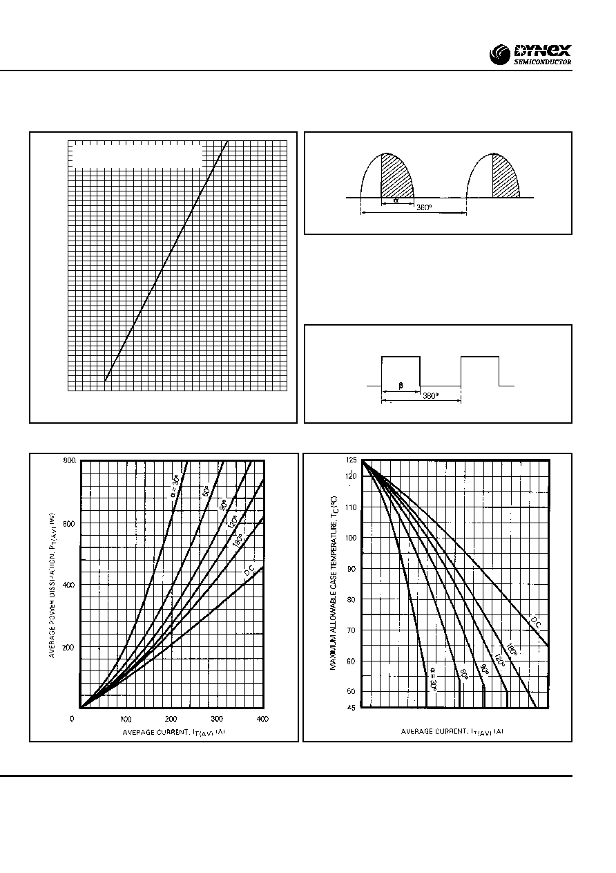
CURVES
SINUSOIDAL CURRENT WAVEFORM
RECTANGULAR CURRENT WAVEFORM
Fig.3 Maximum on-state power dissipation for sinusoidal
current waveform
Fig.2 Maximum (limit) on-state characteristics
Fig.4 Maximum allowable case temperature for sinusoidal
current waveform
Instantaneous on-state current, I
T
- (A)
0
2.0
4.0
6.0
Instantaneous on-state voltage, V
T
- (V)
0
1000
2000
3000
4000
5000
Measured under pulse conditions
T
j
= 125∞C

5/8
TK36
www.dynexsemi.com
Fig.5 Maximum on-state power dissipation for rectangular
current waveform
Fig.6 Maximum allowable case temperature for rectangular
current waveform
Fig.7 Gate trigger characteristics
Fig.8 Transient thermal impedance - junction to case