 | –≠–ª–µ–∫—Ç—Ä–æ–Ω–Ω—ã–π –∫–æ–º–ø–æ–Ω–µ–Ω—Ç: V3022 | –°–∫–∞—á–∞—Ç—å:  PDF PDF  ZIP ZIP |
R
V3022
Copyright © 2004, EM Microelectronic-Marin SA
1
www.emmicroelectronic.com
Very Low Power 8-Bit 32 kHz RTC Module with Digital
Trimming and High Level Integration
Description
The V3022 is a low power CMOS real time clock with a
built in crystal. Standby current is typically 1.2 µA and the
access time is 50 ns. The interface is 8 bits with
multiplexed address and data bus. Multiplexing of
address and data is handled by the input line A /D. There
are no busy flags in the V3022, internal time update
cycles are invisible to the user's software. Time data can
be read from the V3022 in 12 or 24 hour data formats. An
external signal puts the V3022 in standby mode. Even in
standby, the V3022 pulls the IRQ pin active low on an
internal alarm interrupt. Calendar functions include leap
year correction and week number calculation. Time
precision can be achieved by digital trimming.
Applications
Industrial controllers
Alarm systems with periodic wake up
PABX and telephone systems
Point of sale terminals
Automotive electronics
Features
Built-in crystal with digital trimming and temperature
compensation facilities
50 ns access time with 50 pF load capacitance
Standby on power down typically 1.2 µA
Wide voltage range, 2.0V to 5.5V
Universal interface compatible with both Intel and
Motorola
Simple 8 bit interface with no delays or busy flags
Power fail input disables during power up / down of
reset
Bus can be in tri-state in power fail mode
12 or 24 hour data formats
Time to 1/100 of a second
Leap year correction and week number calculation
Alarm and timer interrupts
Programmable interrupts: 10 ms, 100 ms, s or min
Sleep mode capability
Alarm programmable up to one month
Timer measures elapsed time up to 24 hours
Temperature range: -40∞C to +85∞C
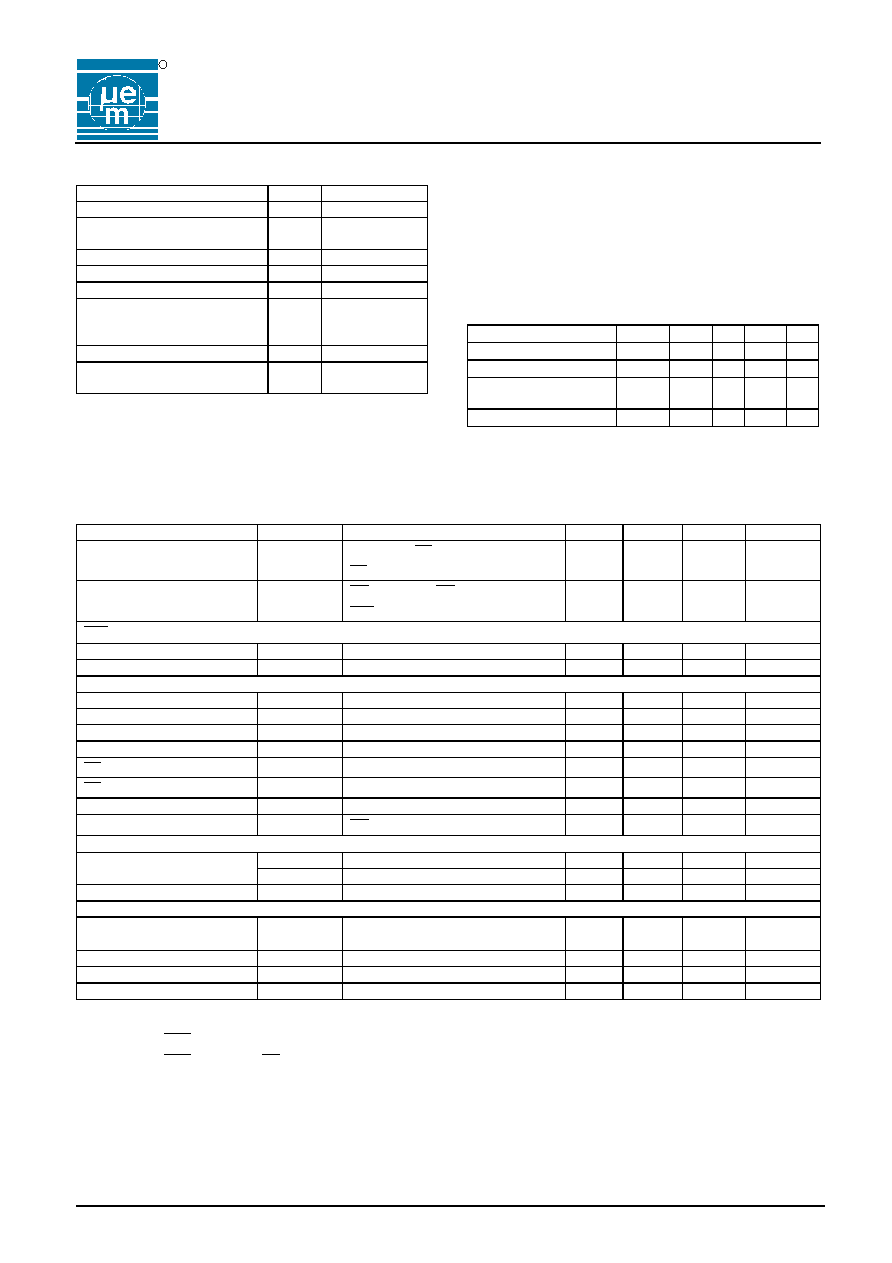
Package SO28
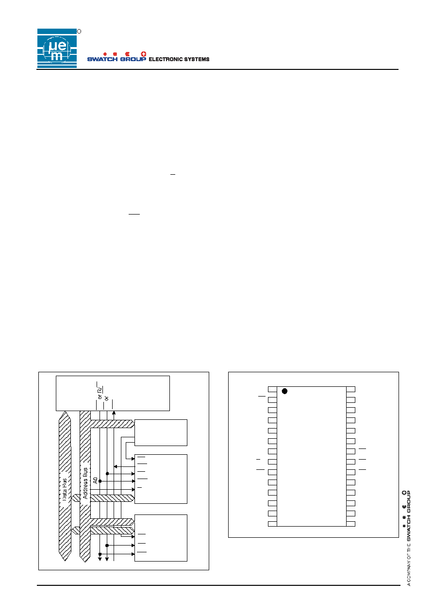
Typical Operating Configuration
Address
Decoder
V3022
CS
RD
WR
AD0 to AD7
CS
RD
WR
CPU
RD
DS
WR
W
IRQ
/D
A
IR
Q
Fig.
1
Pin Assignment
SO28
V3022
TEST
AD0
AD1
NC
AD2
AD3
A/D
IRQ
PF
V
SS
V
SS
V
SS
V
SS
V
SS
NC
AD6
AD5
NC
AD4
RD
WR
CS
AD7
V
DD
V
DD
V
DD
V
DD
V
DD
Fig.
2
EM MICROELECTRONIC -
MARIN SA
R
V3022
Copyright © 2004, EM Microelectronic-Marin SA
2
www.emmicroelectronic.com
Absolute Maximum Ratings
Parameter Symbol
Conditions
Maximum voltage at V
DD
V
DDmax
V
SS
+ 7.0V
Maximum voltage at remaining
pins
V
max
V
DD
+ 0.3V
Min. voltage on all pins
V
min
V
SS
≠ 0.3V
Maximum storage temperature T
STOmax
+125∞C
Minimum storage temperature T
STOmin
-55∞C
Maximum electrostatic
discharge to MIL-STD-883C
method 3015.7 with ref. to V
SS
V
Smax
1000V
Maximum soldering conditions T
Smax
250∞C x 10s
Shock resistance
5000 g.
0.3ms, Ω sine
Table 1
Stresses above these listed maximum ratings may cause
permanent damages to the device. Exposure beyond
specified operating conditions may affect device reliability
or cause malfunction.
Handling Procedures
This device has built-in protection against high static
voltages or electric fields; however, anti-static precautions
must be taken as for any other CMOS component. Unless
otherwise specified, proper operation can only occur when
all terminal voltages are kept within the voltage range.
Unused inputs must always be tied to a defined logic
voltage level.
Operating Conditions
Parameter Symbol
Min
Typ
Max
Unit
Operating temperature
T
A
-40 +85
∞C
Logic supply voltage
V
DD
2.0
5.0
5.5 V
Supply voltage dv/dt
(power-up & down)
dv/dt 6
V/µs
Decoupling capacitor
100
nF
Table 2
Electrical Characteristics
V
DD
= 5.0V ±10%, V
SS
= 0V, T
A
=-40 to +85∞C, unless otherwise specified
Parameter Symbol
Test
Conditions Min
Typ
Max
Unit
Standby current (note 1)
I
DD
V
DD
= 3 V, PF = 0
PF
= 0
1.2
2
10
15
µA
µA
Dynamic current (note 2)
I
DD
CS
= 4 MHz, RD = V
SS
WR
= V
DD
1.5
mA
IRQ
(open drain)
Output low voltage
V
OL
I
OL
= 8 mA
0.4
V
Output low voltage
V
OL
I
OL
= 1 mA, V
DD
= 2 V
0.4
V
Inputs and Outputs
Input logic low
V
IL
T
A
= +25∞C
0.2 V
DD
V
Input logic high
V
IH
T
A
= +25∞C
0.8 V
DD
V
Output logic low
V
OL
I
OL
= 6 mA
0.4
V
Output logic high
V
OH
I
OH
= 6 mA
2.4
V
PF
activation voltage
V
PFL
0.5
V
DD
V
PF
hysteresis
V
H
100
mV
Input leakage
I
IN
V
SS
< V
IN
< V
DD
10
1000
nA
Output tri-state leakage
I
TS
CS
= 1
10 1000 nA
Oscillator Characteristics
Starting voltage
V
STA
T
A
+25∞C
2
V
V
STA
2.5
V
Start-up time
T
STA
1
s
Frequency Characteristics
Frequency tolerance
f/f
TA = +25∞C addr. 10 hex = 00 hex
150 210
(note 4)
251 ppm
Frequency stability
f
sta
2.0
V
DD
5.5 V (note 3)
1
5
ppm/V
Temperature stability
t
sta
addr. 10 hex = 00 hex
see Fig.5
ppm
Aging t
ag
T
A
= +25∞C, first year
±5
ppm/year
Table 3
Note 1
:
With PFO = 0 (V
SS
) all I/O pads can be tri-state, tested.
With
PFO
= 1 (V
DD
), CS = 1 (V
DD
) and all other I/O pads fixed to V
DD
or V
SS
: same standby current, not tested.
Note 2
: All other inputs to V
DD
and all outputs open.
Note 3
: At a give temperature.
Note 4
: See Fig. 4

R
V3022
Copyright © 2004, EM Microelectronic-Marin SA
3
www.emmicroelectronic.com
Typical Standby Current at V
DD
= 5 V
Fig. 3
Typical Frequency on IRQ
Fig. 4
Module Characteristic
O
F
F
= -0.038
2
C
ppm
∞
(T ≠ T
O
)
2
± 10%
F/F
O
=
the ratio of the change in frequency to the
nominal value expressed in ppm (it can be
thought of as the frequency deviation at any
temperature)
T
=
the temperature of interest in ∞C
T
O
=
the turnover temperature (25 ± 5∞C)
To determine the clock error (accuracy) at a given
temperature, add the frequency tolerance at 25∞C to the
value obtained from the formula above.
Fig. 5
R
V3022
Copyright © 2004, EM Microelectronic-Marin SA
4
www.emmicroelectronic.com
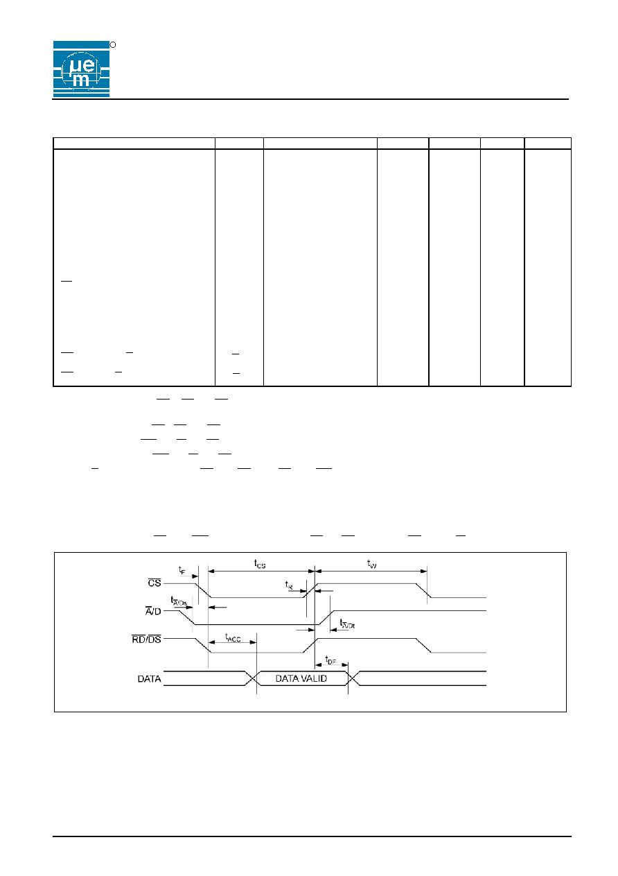
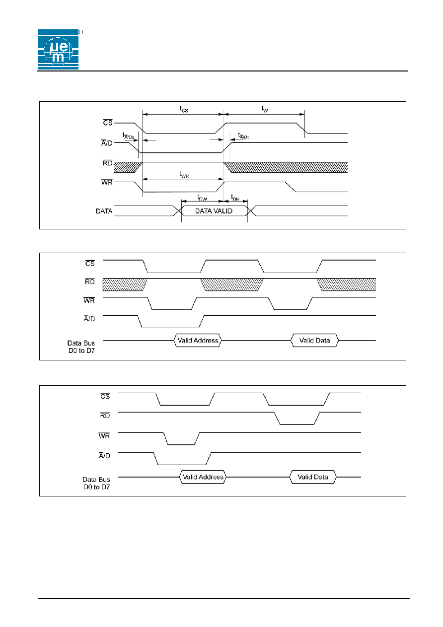
Timing Characteristics (standard temperature range)
V
DD
= 5.0 ±10%, V
SS
= 0V and T
A
=-40 to +85∞C
Parameter Symbol
Test
Conditions
Min.
Typ.
Max.
Unit
Chip select duration, write cycle
t
CS
50
ns
Write pulse duration
t
WR
50
ns
Time between two transfers
t
W
100
ns
RAM access time (note 1)
t
ACC
C
LOAD
= 50pF
50
60
ns
Data valid to Hi-impedance (note 2)
t
DF
10
30
40
ns
Write data settle time (note 3)
t
DW
50
ns
Data hold time (note 4)
t
DH
10
ns
Advance write time
t
ADW
10
ns
PF
response delay
t
PF
100 ns
Rise time (all timing waveform
signals)
t
R
200 ns
Fall time (all timing waveform
signals)
t
F
200 ns
CS delay after A /D (note 5)
t A
/Ds
5
ns
CS delay to A /D
t A
/Dt
10
ns
Table 4
Note 1
: t
ACC
starts from RD , ( DS ) or CS , whichever activates last
Typically,
t
ACC
= 5 + 0.9 C
EXT
in ns; where C
EXT
(external parasitic capacitance) is in pF
Note 2
: t
DF
starts from RD ( DS ) or CS , whichever deactivates first
Note 3
: t
DW
ends at WR (R/ W ) or CS , whichever deactivates first
Note 4
: t
DH
starts from WR (R/ W ) or CS , whichever deactivates first
Note 5
: A /D must come before a CS and RD or a CS and WR combination. The user has to guarantee this.
Timing Waveforms
Read Timing for Intel ( RD and WR Pulse) and Motorola ( DS or RD pin tied to CS and R/ W )
Fig. 6a
R
V3022
Copyright © 2004, EM Microelectronic-Marin SA
5
www.emmicroelectronic.com
Intel Interface
Write Timing
Fig. 6b
Write
Fig. 6c
Read
Fig. 6d