This Data Sheet may be revised by subsequent versions ©2005 Eon Silicon Solution, Inc., www.essi.com.tw
or modifications due to changes in technical specifications.
1
EN29LV640
Rev. B, Issue Date: 2005/10/24
FEATURES
∑
Single power supply operation
- Full voltage range: 2.7 to 3.6 volts for read,
erase and program operations
∑
Low power cons
umption (typical values at 5
MHz)
- 9 mA typical active read current
- 20 mA typical program/erase current
- Less than 1
µ
A current in standby or automatic
sleep mode.
∑
JEDEC standards compatible
- Pinout and software compatible with single-
power supply Flash standard
∑
Manufactured on 0.18
m process
technology
∑
Flexible Sector Architecture:
-
One hundred and twenty-eight 32K-Word /
64K-byte sectors.
∑
Minimum 100K program/erase endurance
cycles.
∑
High performance for program and erase
- Word program time: 8µs typical
- Sector Erase time: 500ms typical
- Chip Erase time: 64s typical
∑
Package Options
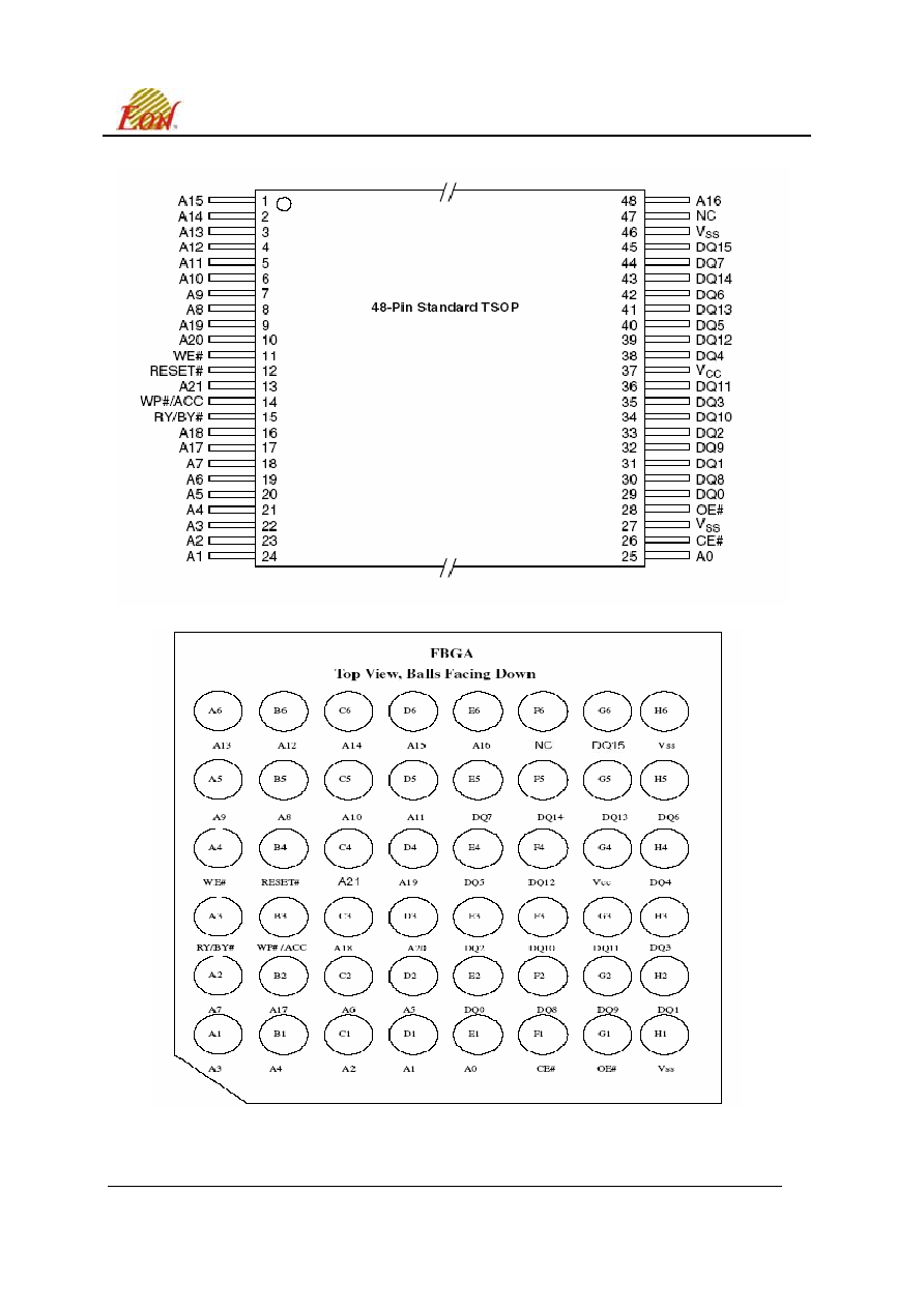
- 48-pin TSOP
- 48-ball FBGA
Software features:
∑
Sector Group Protection
- Provide locking of sectors to prevent program
or erase operations within individual sectors
- Additionally, temporary Sector Group
Unprotect allows code changes in previously
protected sectors.
∑
Standard DATA# polling and toggle bits
feature
∑
Unlock Bypass Program command supported
∑
Sector Erase Suspend / Resume modes:
Read and program another Sector during
Sector Erase Suspend Mode
∑
Support JEDEC Common Flash Interface
(CFI).
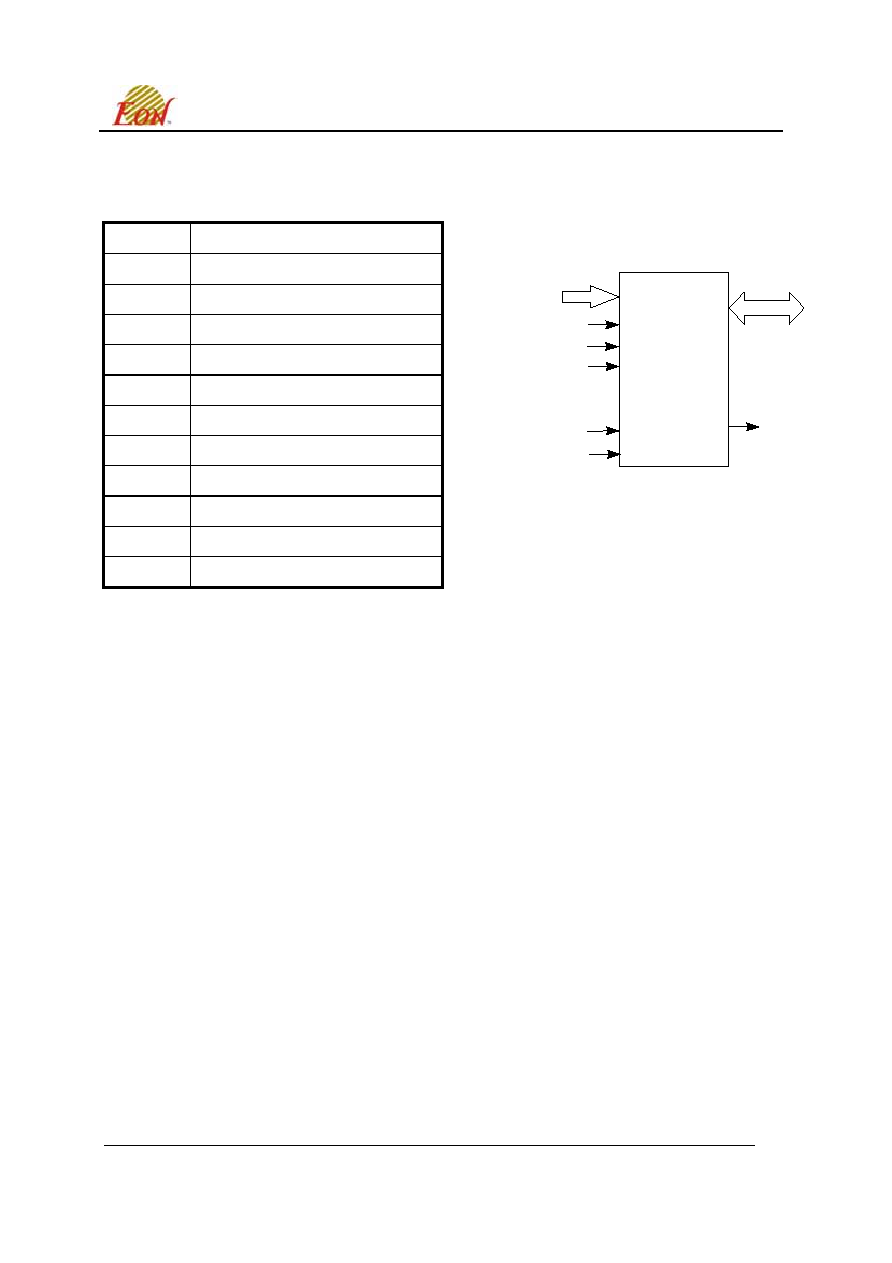
Hardware features:
∑
Pin compatible to lower density, easy
replacement for code expansion.
∑
RESET# hardware reset pin
- Hardware method to reset the device to read
mode.
∑
WP#/ACC input pin
- Write Protect (WP#) function allows
protection of first or last 32K-word sector,
regardless of previous sector protect status
- Acceleration (ACC) function provides
accelerated program times
GENERAL DESCRIPTION
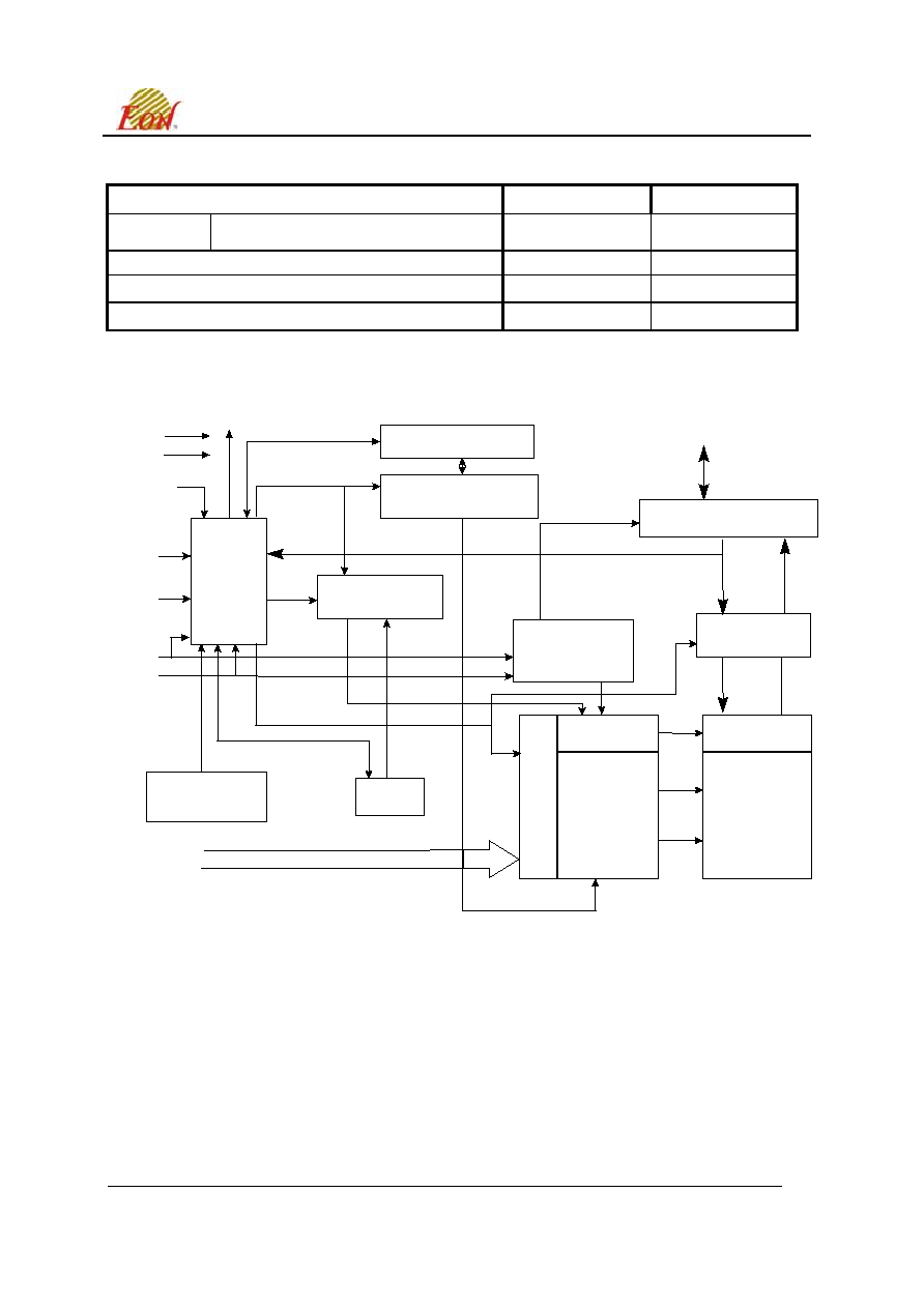
The EN29LV640H/L / EN29LV640U is a 64-Megabit ( 4Mx16 ), electrically erasable, read/write non-
volatile flash memory. Any word can be programmed typically in 8µs. This device is entirely
command set compatible with the JEDEC single-power-supply Flash standard.
The EN29LV640H/L / EN29LV640U is designed to allow either single Sector or full Chip erase
operation, where each Sector Group can be protected against program/erase operations or
temporarily unprotected to erase or program. The device can sustain a minimum of 100K
program/erase cycles on each Sector.
EN29LV640
64 Megabit (4M x 16-bit ) CMOS 3.0 Volt-only,
Uniform Sector Flash Memory
This Data Sheet may be revised by subsequent versions ©2005 Eon Silicon Solution, Inc., www.essi.com.tw
or modifications due to changes in technical specifications.
5
EN29LV640
Rev. B, Issue Date: 2005/10/24
ORDERING INFORMATION
EN29LV640 H
90 T C P
PACKAGING CONTENT
(Blank) = Conventional
P = Pb Free
TEMPERATURE RANGE
I = Industrial (-40
∞
C to +85
∞
C)
C = Commercial (0
∞
C to +70
∞
C)
PACKAGE
T = 48-pin TSOP
B = 48-Ball Fine Pitch Ball Grid Array (FBGA)
0.80mm pitch
SPEED OPTION
See Product Selector Guide and Valid Combinations
SECTOR for WRITE PROTECT (WP#/ACC=0)
H = highest address sector protected
L
=
lowest
address
sector
protected
BASE PART NUMBER
EN29LV640 / EN29LV640U
64 Megabit(4M x 16-Bit) Uniform Sector Flash
3V Read, Erase and Program
PRODUCT SELECTOR GUIDE
Valid Combinations
Vcc
EN29LV640H
≠
90
EN29LV640L
≠
90
TI, TC
BI,BC
V
cc
= 2.7V-3.6V