47
Real time clock module
Absolute Max. rating
Specifications (characteristics)
Operating range
Frequency characteristics
Electrical characteristics
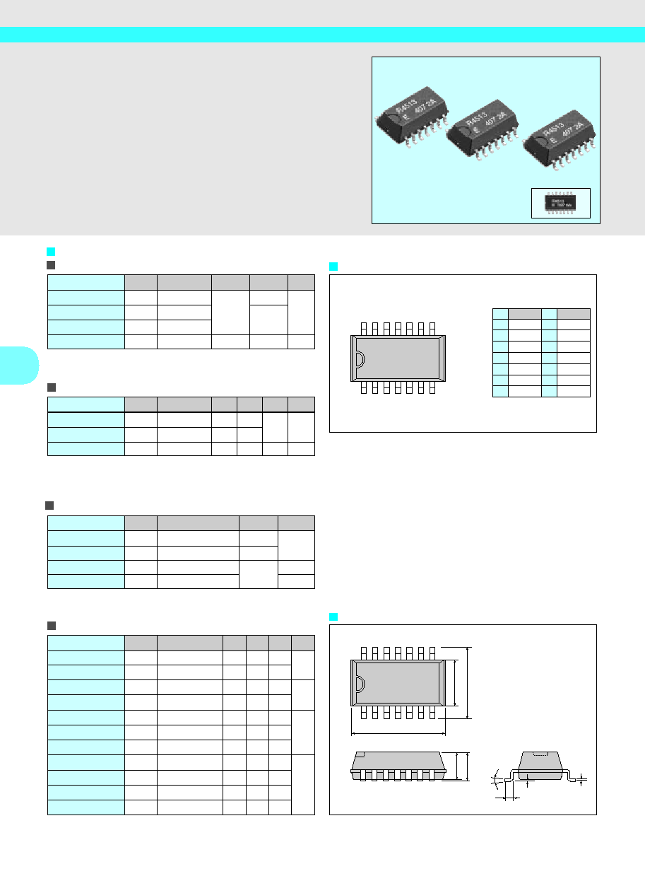
External dimensions
(Unit: mm)
R4513
607 6A
E
7.4
±
0.2
3.2
±
0.1
5.0
3.1
10.1
±
0.2
Terminal connection
0.15
0.6
0.05 min.
No.
1
2
3
4
5
6
7
Pin terminal
N.C
DATA
STD.P
N.C
N.C
V
DD
N.C
No.
14
13
12
11
10
9
8
Pin terminal
N.C
CLK
CE
N.C
N.C
GND
N.C
1 2 3
4 5 6 7
14 13 12 11 10 9 8
0∞ to
10∞
∑ Builtin crystal unit allows adjustment-free efficient operation.
∑ Using a serial interface, controllable only three signal lines.
∑ Automatic leap year correction.
∑ 30 second adjustment, available.
∑ Wide operating voltage from 2.7V to 5.5V.
SERIAL-INTERFACE REAL TIME CLOCK MODULE
RTC-4513
Item
Power source voltage
Input voltage
Output voltage
Storage temperature
Symbol
V
DD
V
IN
V
OUT
T
STG
Condition
V
DD
-GND
Min.
-0.3
-55
Max.
7.0
V
DD
+0.3
+125
Unit
V
∞C
Item
Operating voltage
Date holding voltage
Operating temperature
Symbol
V
DD
V
CLK
T
OPR
Condition
Min.
2.7
2.0
-40
Typ.
5.0
Max.
5.5
+85
Unit
V
∞C
Item
Frequency tolerance
Frequency temperature
characteristics
f-V characteristics
Aging
Symbol
f/fo
Top
f
V
fa
Condition
Ta=25∞C, V
DD
=3V
-10 to +70∞C
Ta=25∞C, V
DD
=2.0 to 5.5V
First year Ta=25∞C, V
DD
=3V
Range
0±25
+10/-120
±5
Unit
ppm
ppm/V
ppm/year
Item
"H" input voltage
"L" input voltage
Input leak current 1
Input leak current 2
"L"
output voltage 1
"H"
output voltage
"L"
output voltage 2
Off leak current
Current consumption 1
Current consumption 2
Current consumption 3
Symbol
V
IH
V
IL
I
IL1
I
IL2
V
OL1
V
OH
V
OL2
I
OFLK
I
DD1
I
DD2
I
DD3
Condition
--
--
V
IN
=V
DD
/GND (CE,CLK)
V
IN
=V
DD
/GND (DATA)
I
O
=1mA (DATA)
I
O
=-400µA (DATA)
I
O
=1mA (STD.P)
V
O
=V
DD
V
DD
=5V, V
IN
(CE) =0V
V
DD
=3V, V
IN
(CE) =0V
V
DD
=2V, V
IN
(CE) =0V
Min.
0.8V
DD
0.8V
DD
Typ.
10.0
2.5
1.0
Max.
0.2V
DD
1/-1
10/-10
0.2V
DD
0.2V
DD
10.0
20.0
5.0
2.0
Unit
V
µA
V
µA
Actual size
