35
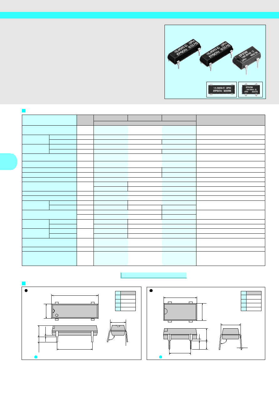
Crystal oscillator
(Unit: mm)
5.3max.
0.2min.
0.25
7.62
2.54min.
7.62
# 4
# 1
# 5
# 8
13.7max.
6.6
100.0000 C
9357B
EPSON
2PH
No.
1
4
5
8
OE or ST
GND
OUT
V
DD
No.
1
7
8
14
OE or ST
GND
OUT
V
DD
90 to 105�
90 to 105�
External dimensions
Specifications (characteristics)
(Unit: mm)
Pin terminal
Pin terminal
19.8max.
6.36
2.54min.
5.3max.
0.2min.
15.24
7.62
# 14 # 8
# 1 # 7
9357B
16.0000 C
EPSON
2PH
SG-8002DB series
SG-8002DC series
PROGRAMMABLE HIGH-FREQUENCY CRYSTAL OSCILLATOR
SG-8002DB/ DC series
Item
Output frequency range
Power source
voltage
Temperature
range
Soldering condition
Frequency stability
Current consumption
Output disable current
Standby current
Duty
High output voltage
Low output voltage
Output load
condition (fan out)
Output enable/disable input voltage
Output rise time
Output fall time
Oscillation start up time
Aging
Shock resistance
Symbol
f
0
V
DD
-GND
V
DD
T
STG
T
OPR
T
SOL
f/f
0
Iop
I
OE
I
ST
t
w
/
t
V
OH
V
OL
N
C
L
V
IH
V
IL
t
TLH
t
THL
t
OSC
fa
S.R.
TTL
C-MOS
C-MOS level
TTL level
C-MOS level
TTL level
PT/ST PH/SH PC/SC
Specifications
-0.5V to +7.0V
5.0V�0.5V 3.3
� 0.3V
-55�C to +125�C
-20�C to +70�C (-40�C to +85�C) -40�C to +85�C
Twice at under 260�C within 10 sec.
or under 230�C within 3 min.
B: �50ppm C: � 100ppm M: �100ppm(-40�C to +85�C)
45mA max. 28mA max.
30mA max. 16mA max.
-- 40% to 60%
40% to 60% --
V
DD
-0.4V min.
0.4V max.
5TTL max.
--
15pF max. 25pF max. 15pF max.
2.0V min. 0.7
�
V
DD
min.
0.8V max. 0.2
�
V
DD
max.
-- 4ns
max.
4ns max. --
-- 4ns
max.
4ns max. --
10ms max.
�5ppm/year max.
�20ppm max.
Remarks
3.0V �0.3V: f
0
66.7MHz(PC/SC)
Refer to page 4."Frequency range"
-20�C to +70�C
No load condition, Max. frequency range
OE=GND(PT, PH, PC)
ST=GND(ST, SH, SC)
C-MOS load: 1/2V
DD
level
TTL load: 1.4V level
I
OH
=-16mA(PT /ST, PH /SH),-8mA(PC /SC)
I
OL
= 16mA(PT /ST, PH /SH), 8mA(PC /SC)
Max. frequency and max. operating voltage range
ST
_
, OE terminal
C-MOS load: 20
%
80
%
V
DD
TTL load: 0.4V
2.4V
C-MOS load: 80
%
20
%
V
DD
TTL load: 2.4V
0.4V
Time at minimum operating voltage to be 0 sec.
Ta= 25�C, V
DD
= 5.0V/3.3V(PC/SC)
Three drops on a hard board from 75 cm or
excitation test with 3000G x 0.3ms x 1/2sine
wave in 3 directions
Note: � Please contact us for inquiries about operating temperature(-40�C to +85�C), usable frequencies, duty and output load conditions.
Checking possible by the Frequency Checking Program.
Max. supply voltage
Operating voltage
Storage temperature
Operating temperature
50�A max.
� Wide frequency output by PLL technology.
� Quick delivery of samples and short lead mass production time.
� Excellent shock resistance and environmental capability.
� Output enable function (OE) and stand-by function (ST) can be
used for low current consumption applications.
� Pin compatible with full size and half size.
8002 PROM Writer available to purchase.(Type:PRW-8000A3-M01)
Please contact EPSON or local sales representative.
1.0000 MHz to
125.0000 MHz
Actual size
http://www.epson.co.jp/CRYSTAL/
SG-8002DB SG-8002DC
(Wired-or connection & Jitter specification, please refer to page 13.) (Wired-or connection & Jitter specification, please refer to page 13.)
THE CRYSTALMASTER
NOTICE
SEIKO EPSON CORP. QUARTZ DEVICE DIVISION acquired ISO9001 and ISO14001 certification
by B.V.Q. I. (Bureau Veritas Quality International) .
ISO9001 in October, 1992.
ISO14001 in November,1997.
No part of this material may be reproduced or duplicated in any form or by any means without the written permission of Seiko
Epson. Seiko Epson reserves the right to make changes to this material without notice. Seiko Epson does not assume any
liability of any kind arising out of any inaccuracies contained in this material or due to its application or use in any product or
circuit and, further, there is no representation that this material is applicable to products requiring high level reliability, such as,
medical products. Moreover, no license to any intellectual property rights is granted by implication or otherwise, and there is no
representation or warranty that anything made in accordance with this material will be free from any patent or copyright
infringement of a third party. This material of portions there may contain technology or the subject relating to strategic products
under the control of the Foreign Exchange and Foreign Trade Control Law of Japan and may require an export license from the
Ministry of International Trade and Industry or other approval from another government agency.
ENERGY SAVING EPSON
Our concept of Energy Saving technology conserves
resources by blending the essence of these three efficiency
technologies. The essence of these technologies is repre-
sented in each of the products that we provide to our cus-
tomers.
In the industrial sector, leading priorities include mea-
sures to counter the greenhouse effect by reducing CO2,
measures to preserve the global environ-
ment, and the development of energy-
efficient products. Environmental
problems are of global concern, and
although the contribution of energy-
saving technology developed by
EPSON may appear insignificant,
we seek to contribute to the develop-
ment of energy-saving products by our
customers through the utilization of our electronic devices.
EPSON is committed to the conservation of energy, both
for the sake of people and of the planet on which we live.
EPSON offers effective savings to its customers through
a wide range of electronic devices, such as semiconductors,
liquid crystal display (LCD) modules, and crystal devices.
These savings are achieved through a sophisticated melding
of three different efficiency technologies.
Power saving technology
provides low power con-
sumption at low voltages.
Space saving technology
provides further reductions
in product size and weight
through super-precise pro-
cessing and high-density
assembly technology.
Time saving technology
shortens the time required
for design and development
on the customer side and
shortens delivery times.
Energy Saving
Power Saving
Space Saving
Time Saving
Resource
Saving