 | –≠–ª–µ–∫—Ç—Ä–æ–Ω–Ω—ã–π –∫–æ–º–ø–æ–Ω–µ–Ω—Ç: PTF10133 | –°–∫–∞—á–∞—Ç—å:  PDF PDF  ZIP ZIP |

e
1
RF Specifications
(100% Tested)
Characteristic
Symbol
Min
Typ
Max
Units
Gain
(V
DD
= 28 V, P
OUT
= 85 W, I
DQ
= 1.0 A, f = 894 MHz)
G
ps
12.5
13.5
--
dB
Power Output at 1 dB Compression
(V
DD
= 28 V, I
DQ
= 1.0 A, f = 894 MHz)
P-1dB
85
90
--
Watts
Drain Efficiency
(V
DD
= 28 V, P
OUT
= 85 W, I
DQ
= 1.0 A, f = 894 MHz)
h
45
50
--
%
Load Mismatch Tolerance
(V
DD
= 28 V, P
OUT
= 85 W, I
DQ
= 1.0 A, f = 894 MHz
Y
--
--
10:1
--
--all phase angles at frequency of test)
All published data at T
CASE
= 25∞C unless otherwise indicated.
Description
The PTF 10133 is an internally matched 85 watt LDMOS FET
intended for cellular, GSM and D-AMPS applications. This device
operates at 50% efficiency with 13.5 dB of gain. Full gold metallization
ensures excellent device lifetime and reliability.
PTF 10133
85 Watts, 860≠960 MHz
GOLDMOS
TM
Field Effect Transistor
10133
A-1234569947
0
20
40
60
80
100
120
0
1
2
3
4
5
6
Input Power (Watts)
Ou
tp
u
t
P
o
wer
(Watts)
0
10
20
30
40
50
60
E
fficien
cy (%
)
V
DD
= 28.0 V
I
DQ
= 1.0 A
f = 894 MHz
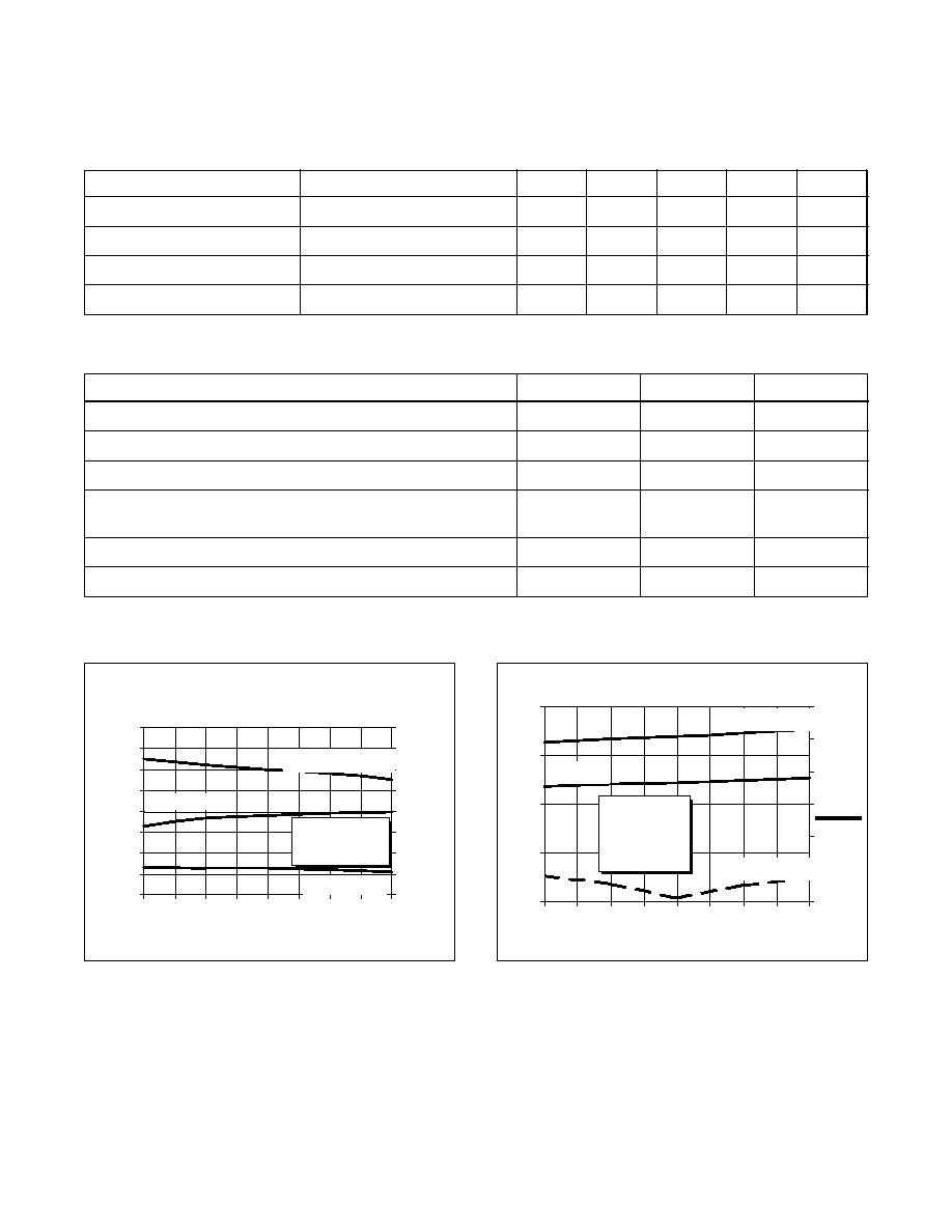
Typical Output Power vs. Input Power
Output Pow er
Efficiency
Package 20248
∑
INTERNALLY MATCHED
∑
Performance at 894 MHz, 28 Volts
- Output Power = 85 Watts
- Power Gain = 13.5 dB Typ
- Efficiency = 50% Typ
∑
Full Gold Metallization
∑
Silicon Nitride Passivated
∑
Excellent Thermal Stability
∑
100% Lot Traceability
2
PTF 10133
e
10
11
12
13
14
15
16
17
18
860 865 870 875 880 885 890 895 900
Frequency (MHz)
Gain
40
50
60
70
80
90
100
110
120
Output P
o
wer & E
fficienc
y
V
DD
= 28 V
I
DQ
= 1.0 A
Typical P
OUT
, Gain & Efficiency
(at P-1dB)
vs. Frequency
Output Pow er (W)
Efficiency
Gain
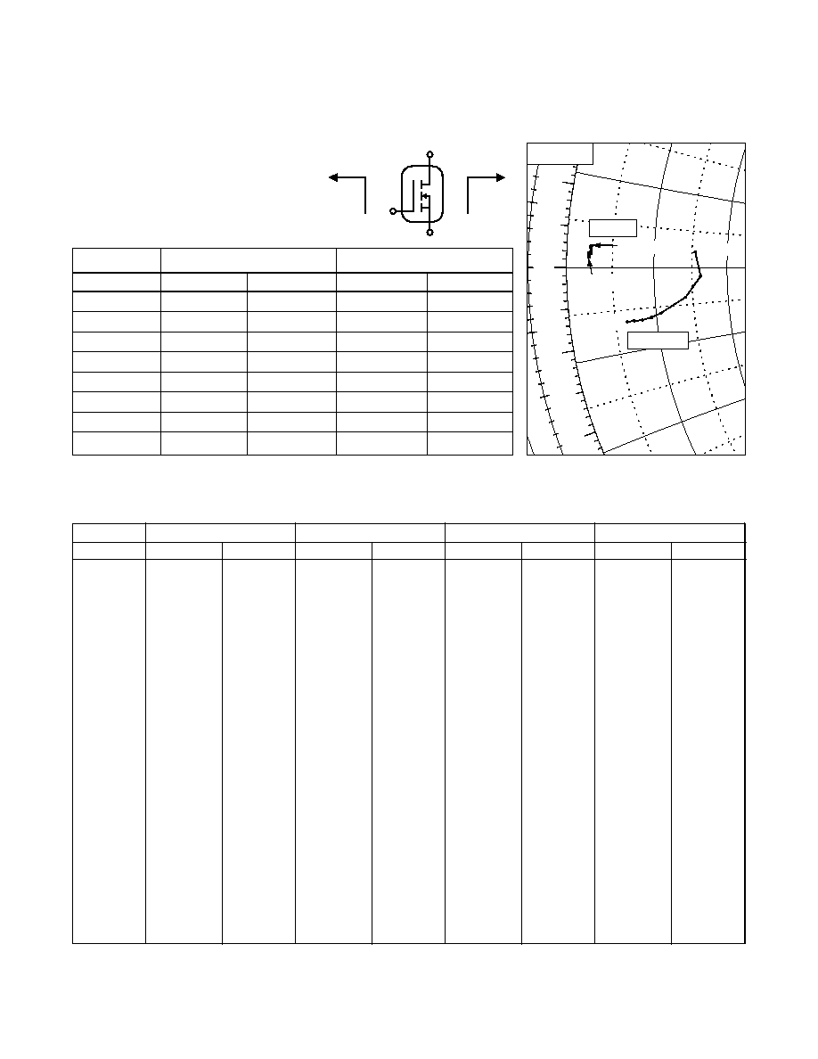
Broadband Test Fixture Performance
4
8
12
16
20
860 865
870 875 880 885
890 895 900
Frequency (MHz)
Gai
n (dB
)
0
10
20
30
40
50
60
V
DD
= 28 V
I
DQ
= 1.0 A
P
OUT
= 85 W
Gain (dB)
Return Loss (dB)
Ef ficiency (%)
E
ffi
ci
enc
y
R
e
turn Los
s
0
-10
-20
Electrical Characteristics
(100% Tested)
Characteristic
Conditions
Symbol
Min
Typ
Max
Units
Drain-Source Breakdown Voltage
V
GS
= 0 V, I
D
= 25 mA
V
(BR)DSS
65
--
--
Volts
Drain-Source Leakage Current
V
DS
= 28 V, V
GS
= 0 V
I
DSS
--
--
1.0
mA
Gate Threshold Voltage
V
DS
= 10 V, I
D
= 75 mA
V
GS(th)
3.0
--
5.0
Volts
Forward Transconductance
V
DS
= 10 V, I
D
= 3 A
g
fs
--
3.0
--
Siemens
Maximum Ratings
Parameter
Symbol
Value
Unit
Drain-Source Voltage
V
DSS
65
Vdc
Gate-Source Voltage
V
GS
±20
Vdc
Operating Junction Temperature
T
J
200
∞C
Total Device Dissipation
P
D
205
Watts
Above 25∞C derate by
1.18
W/∞C
Storage Temperature Range
T
STG
≠40 to +150
∞C
Thermal Resistance (T
CASE
= 70∞C)
R
q
JC
0.85
∞C/W
Typical Performance

3
PTF 10133
e
Output Power vs. Supply Voltage
40
50
60
70
80
90
100
110
24
26
28
30
32
34
36
Supply Voltage (Volts)
Output P
o
wer
(W
atts)
I
DQ
= 1.0 A
f = 894 MHz
Capacitance vs. Supply Voltage *
0
50
100
150
200
250
300
0
10
20
30
40
Supply Voltage (Volts)
Cds & Cgs (pF
)
0
8
16
24
32
40
48
Crss (pF)
C
gs
C
ds
C
rss
V
GS
= 0 V
f = 1 MHz
-70
-60
-50
-40
-30
-20
-10
0
20
40
60
80
100
Output Power (Watts-PEP)
IM
D (d
Bc)
V
DD
= 28 V, I
DQ
=1A
f
1
= 894 MHz, f
2
= 894.1 MHz
Intermodulation Distortion vs. Output Power
(as measured in a broadband circuit)
3rd Order
7th
5th
Power Gain vs. Output Power
11
12
13
14
15
16
0.1
10.0
1000.0
Output Power (Watts)
P
o
wer Gai
n
(dB)
V
DD
= 28 V
f = 894 MHz
I
DQ
= 1.0
I
DQ
= 500
I
DQ
= 250
* This part is internally matched. Measurements of the
finished product will not yield these figures.
Bias Voltage vs. Temperature
0.95
0.96
0.97
0.98
0.99
1.00
1.01
1.02
1.03
-20
30
80
130
Temp. (∞C)
Bias Voltage (V)
0.86
2.5
4.16
5.8
7.42
9.06
Voltage normalized to 1.0 V
Series show current (A)
4
PTF 10133
e
Frequency
Z Source
W
Z Load
W
MHz
R
jX
R
jX
860
3.2
-3.2
1.3
1.2
870
3.6
-3.2
1.3
1.1
880
4.1
-3.2
1.3
0.9
890
4.7
-3.1
1.3
0.8
900
5.3
-2.9
1.2
0.8
925
7.0
-2.0
1.2
0.7
942
8.1
-0.6
1.2
0.7
960
7.7
1.1
1.2
0.6
Z Source
Z Load
G
S
D
Impedance Data
(V
DD
= 28 V, P
OUT
= 85 W, I
DQ
= 1.0 A)
0.
1
0.
2
0.1
0.1
0.2
WA
R
D
G
E
<
--
-
W
A
V
E
L
E
N
G
T
H
S
T
O
W
A
R
D
L
O
A
D
-
0
.
0
Z Load
860 MHz
960 MHz
860 MHz
960 MHz
Z Source
Z
0
= 50
W
Typical Scattering Parameters
(V
DS
= 28 V, I
D
= 2 A per side)
f
S11
S21
S12
S22
(MHz)
Mag
Ang
Mag
Ang
Mag
Ang
Mag
Ang
300
0.980
-178
0.996
15.6
0.010
-85.2
0.994
-177
350
0.982
-179
0.773
12.8
0.008
-85.3
0.993
-177
400
0.983
-180
0.641
9.48
0.006
-85.7
0.992
-178
450
0.989
179
0.545
7.19
0.005
-85.3
0.996
-179
500
0.989
179
0.489
5.48
0.003
-93.7
0.999
-179
550
0.987
179
0.449
2.11
0.002
-74.5
0.995
-179
600
0.983
178
0.425
-0.90
0.002
-64.9
0.996
-179
650
0.982
177
0.414
-4.52
0.001
-68.5
0.998
-180
700
0.980
176
0.405
-10.2
0.001
-55.1
0.997
-180
750
0.972
175
0.419
-14.3
0.001
-88.5
0.997
180
800
0.958
174
0.442
-19.9
0.001
-87.2
0.993
180
850
0.929
171
0.509
-27.5
0.005
-105
0.991
179
900
0.858
168
0.662
-42.4
0.013
-133
0.989
179
950
0.693
173
0.882
-75.9
0.030
174
0.987
179
1000
0.783
-170
0.714
-125
0.028
120
0.993
179
1050
0.918
-172
0.423
-153
0.022
101
0.989
179
1100
0.951
-175
0.261
-167
0.020
89.2
0.982
179
1150
0.974
-177
0.184
-179
0.019
81.8
0.982
178
1200
0.988
-178
0.124
165
0.018
77.9
0.990
178
1250
0.984
-179
0.060
158
0.017
76.7
0.990
178
1300
0.979
-180
0.048
-154
0.018
77.4
0.986
178
1350
0.980
180
0.070
179
0.018
73.9
0.983
178
1400
0.992
180
0.058
166
0.018
74.5
0.990
177
1450
0.991
179
0.049
156
0.019
78.7
0.992
178
1500
0.986
178
0.042
149
0.021
79.7
0.984
178

5
PTF 10133
e
Test Circuit
Test Circuit Schematic for f = 894 MHz
DUT
PTF 10133
LDMOS Field Effect Transistor
l
1
0.040
l
894 GHz
Microstrip 50
W
l
2
0.096
l
894 GHz
Microstrip 50
W
l
3
0.098
l
894 GHz
Microstrip 50
W
l
4
0.073
l
894 GHz
Microstrip 9.29
W
l
5
0.107
l
894 GHz
Microstrip 9.29
W
l
6
0.110
l
894 GHz
Microstrip 6.98
W
l
7
0.250
l
894 GHz
Microstrip 77.9
W
l
8
0.081
l
894 GHz
Microstrip 6.98
W
l
9
0.178
l
894 GHz
Microstrip 50
W
l
10
0.040
l
894 GHz
Microstrip 50
W
C1, C3, C5, C10
Capacitor, 36 pF
ATC 100 B
C2
Capacitor, 4.3 pF
ATC 100 B
C4
Capacitor, 6.2 pF
ATC 100 B
C6
Capacitor, 0.1
m
F, 50 V
Digi-Key P4525-ND
C7
Capacitor, 100
m
F, 50 V
Digi-Key P5182-ND
C8
Capacitor, 2.0 pF
ATC 100 B
C9
Capacitor, 0.6-6 pF
ATC 100 B
R1, R2, R3
Resistor, 220
W
Digi-Key 1KQBK
Circuit Board
e
r
= 4.0, .028 Dielectric Thickness, 1 Oz.
Circuit Board
.028" Dielectric Thickness,
e
r
= 4.0,
AlliedSignal, G200, 2 oz. copper
Components Layout (not to scale)

6
PTF 10133
e
Package Mechanical Specifications
Package 20248
Unless otherwise specified
Pins: 1.Drain 2.Source 3.Gate
all tolerance ±0.005"
Lead Thickness: 0.004 +0.002/-0.001"
Ericsson Microelectronics
RF Power Products
Morgan Hill, CA 95037 USA
Specifications subject to change without notice.
L3
© 1998 Ericsson Inc.
EUS/KR 1301-PTF 10133 Uen Rev. A 12-01-99
1-877-GOLDMOS (465-3667) United States
+46 8 757 4700 International
e-mail: rfpower@ericsson.com
www.ericsson.com/rfpower
Artwork (1 inch
)