 | –≠–ª–µ–∫—Ç—Ä–æ–Ω–Ω—ã–π –∫–æ–º–ø–æ–Ω–µ–Ω—Ç: PTF102027 | –°–∫–∞—á–∞—Ç—å:  PDF PDF  ZIP ZIP |

e
1
RF Specifications
(100% Tested)
Characteristic
Symbol
Min
Typ
Max
Units
Gain
(V
DD
= 26 V, P
OUT
= 40 W, I
DQ
= 250 mA, f = 960 MHz)
G
pe
14.5
15
--
dB
Power Output at 1 dB Compression
(V
DD
= 26 V, I
DQ
= 250 mA, f = 960 MHz)
P-1dB
40
45
--
Watts
Drain Efficiency
(V
DD
= 26 V, P
OUT
= 40 W, I
DQ
= 250 mA, f = 960 MHz)
h
40
53
--
%
Load Mismatch Tolerance
(V
DD
= 26 V, P
OUT
= 40 W, I
DQ
= 250 mA, f = 960 MHz
Y
10:1
--
--
--
--all phase angles at frequency of test)
All published data at T
CASE
= 25∞C unless otherwise indicated.
Description
The PTF 102027 is a 40≠watt GOLDMOS FET intended for EDGE
applications from 925 to 960 MHz. This device operates at 53%
efficiency with 15 dB of gain typical. Full gold metallization ensures
excellent device lifetime and reliability.
PTF 102027
40 Watts, 925≠960 MHz
GOLDMOS
Æ
Field Effect Transistor
102027
1234560050
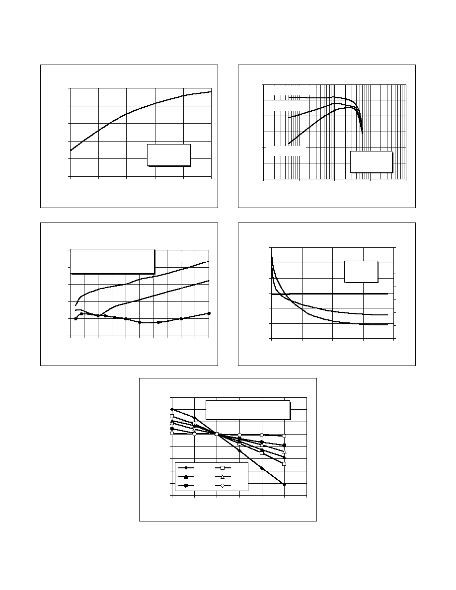
0
10
20
30
40
50
60
70
0.0
0.5
1.0
1.5
2.0
Input Power (Watts)
Power Output (Watts)
0
10
20
30
40
50
60
70
Efficiency (%)
V
DD
= 26 V
I
DQ
= 250 mA
f = 960 MHz
Typical Power Output and Efficiency
vs. Input Power
Efficiency
Power Output
Package 20222
∑
Performance at 960 MHz, 26 Volts
- Output Power = 40 Watts
- Power Gain = 15.0 dB Typical
- Efficiency = 53% Typical
∑
Full Gold Metallization
∑
Excellent Thermal Stability
∑
100% Lot Traceability

2
PTF 102027
e
10
12
14
16
18
20
925
930
935
940
945
950
955
960
Frequency (MHz)
Ga
i
n
20
30
40
50
60
70
V
DD
= 26 V
I
DQ
= 250 mA
Output Power (W)
Efficiency (%)
Gain (dB)
Typical P
OUT
, Gain & Efficiency
(at P-1dB)
vs. Frequency
O
u
tput Pow
e
r
&
Efficiency
Broadband Test Fixture Performance
2
4
6
8
10
12
14
16
18
925
930
935
940
945
950
955
960
Frequency (MHz)
G
a
in (dB)
-10
0
10
20
30
40
50
60
70
V
DD
= 26 V
I
DQ
= 250 mA
P
OUT
= 40 W
Gain
Return Loss (dB)
Efficiency
Efficiency (%)
Return Loss
-15
-30
Electrical Characteristics
(100% Tested)
Characteristic
Conditions
Symbol
Min
Typ
Max
Units
Drain-Source Breakdown Voltage V
GS
= 0 V, I
D
= 25 mA
V
(BR)DSS
65
--
--
Volts
Drain-Source Leakage Current
V
DS
= 26 V, V
GS
= 0 V
I
DSS
--
--
1.0
mA
Gate Threshold Voltage
V
DS
= 10 V, I
D
= 100 mA
V
GS(th)
3.0
--
5.0
Volts
Forward Transconductance
V
DS
= 5 V, I
D
= 3 A
g
fs
--
2.0
--
Siemens
Maximum Ratings
Parameter
Symbol
Value
Unit
Drain-Source Voltage
V
DSS
65
Vdc
Gate-Source Voltage
V
GS
±20
Vdc
Operating Junction Temperature
T
J
200
∞C
Total Device Dissipation
P
D
125
Watts
Above 25∞C derate by
0.714
W/∞C
Storage Temperature Range
T
STG
≠40 to +150
∞C
Thermal Resistance (T
CASE
= 70∞C)
R
q
JC
1.4
∞C/W
Typical Performance
3
PTF 102027
e
25
30
35
40
45
50
20
22
24
26
28
30
Supply Voltage (Volts)
Output Power (Watts)
I
DQ
= 250 mA
f = 960 MHz
Output Power vs. Supply Voltage
Power Gain vs. Output Power
14
15
16
17
0
1
10
100
1000
Output Power (Watts)
Po
we
r Ga
i
n
(d
B)
V
DD
= 26 V
f = 960 MHz
I
DQ
= 250 mA
I
DQ
= 325 mA
I
DQ
= 175 mA
-70
-60
-50
-40
-30
-20
0
5
10
15
20
25
30
35
40
45
50
Output Power (Watts-PEP)
IM
D (dBc
)
V
DD
= 26 V, I
DQ
= 250 mA
f
1
= 959 MHz, f
2
= 960 MHz
Intermodulation Distortion vs. Output Power
(as measured in a broadband circuit)
3rd Order
7th
5th
Capacitance vs. Supply Voltage
0
20
40
60
80
100
120
0
10
20
30
40
Supply Voltage (Volts)
Cds and Cgs (pF)
0
1
2
3
4
5
6
7
Crs
s
C
gs
C
ds
C
rss
V
GS
= 0 V
f = 1 MHz
0.95
0.96
0.97
0.98
0.99
1.00
1.01
1.02
1.03
-20
0
20
40
60
80
100
Case Temperature (∞C)
B
i
as Voltage (V)
0.200
0.692
1.183
1.675
2.167
2.658
Voltage normalized to 1.0 V
Series show current (A)
Gate-Source Voltage vs. Case Temperature

4
PTF 102027
e
Test Circuit Schematic for f = 960 MHz
DUT
PTF 102027
LDMOS Transistor
l
1,
l
9
0.169
l
960 MHz
Microstrip 50
W
l
2
0.020
l
960 MHz
Microstrip 50
W
l
3
0.079
l
960 MHz
Microstrip 50
W
l
4
0.158
l
960 MHz
Microstrip 7.0
W
l
5,
l
6
0.016
l
960 MHz
Microstrip 7.0
W
l
7
0.095
l
960 MHz
Microstrip 10
W
l
8
0.150
l
960 MHz
Microstrip 10
W
l
10
0.047
l
960 MHz
Microstrip 50
W
l
11
0.118
l
960 MHz
Microstrip 50
W
l
12
0.254
l
960 MHz
Microstrip 50
W
l
13
0.315
l
960 MHz
Microstrip 85
W
Frequency
Z Source
W
Z Load
W
MHz
R
jX
R
jX
925
0.770
1.98
2.64
1.28
930
0.750
2.09
2.60
1.38
940
0.700
2.10
2.50
1.57
950
0.650
2.20
2.43
1.78
960
0.625
2.32
2.40
1.98
Test Circuit
Z Source
Z Load
G
S
D
Impedance Data
V
DD
= 26 V, P
OUT
= 40 W, I
DQ
= 250 mA
Z
0
= 10
W
C1, C8
Capacitor, 0.1 µF, 50V
Digi-Key P4525-ND
C2, C3, C9, C12
Capacitor, 36 pF
100B 360
C6, C13
Capacitor, 3.6 pF
100B 3R6
C4, C14
Capacitor, 3.3 pF
100B 3R3
C5, C7
Capacitor, 11 pF
100B 110
C10
Capacitor, 100 µF, 50 V
Digi-Key P5182-ND
C11
Capacitor, 5.1 pF
100B 5R1
J1, J2
Connector, SMA, Female, Panel Mount
Ericsson, #Rpm 513 412/53
R1, R2, R3
Resistor, 220 ohm, 1/4W
Digi-Key 220QBK-ND
PCB
.031" Thick, 2 Oz Copper Both Sides
AlliedSignal, G200
5
PTF 102027
e
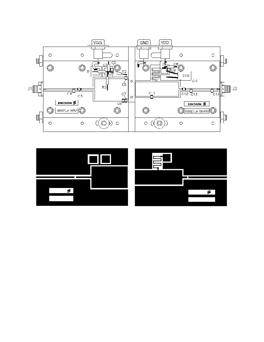
Assembly Diagram (not to scale)
Artwork (not to scale)
10007_A INPUT
ERICSSON
ERICSSON
10007_A OUT PUT
102027_A INPUT
102027_A OUTPUT

6
PTF 102027
e
Case Outline Specifications
Package 20222
Ericsson Inc.
Microelectronics
Morgan Hill, CA 95037 USA
Specifications subject to change without notice.
L3
© 2000, 2001 Ericsson Inc.
EUS/KR 1522-PTF 102027 Uen Rev. A 01-30-01
1-877-GOLDMOS (465-3667) United States
+46 8 757 4700 International
e-mail: rfpower@ericsson.com
www.ericsson.com/rfpower