 | ÐлекÑÑоннÑй компоненÑ: AOD442 | СкаÑаÑÑ:  PDF PDF  ZIP ZIP |
Äîêóìåíòàöèÿ è îïèñàíèÿ www.docs.chipfind.ru
Absolute Maximum Ratings T
A
=25°C unless otherwise noted
Parameter
Symbol
Maximum
Units
Drain-Source Voltage
V
DS
60
V
Gate-Source Voltage
V
GS
±20
V
Continuous Drain
Current
B,G
T
C
=25°C
G
I
D
38
A
T
C
=100°C
B
27
Pulsed Drain Current
I
DM
60
Avalanche Current
C
I
AR
30
A
Repetitive avalanche energy L=0.1mH
C
E
AR
140
mJ
Power Dissipation
B
T
C
=25°C
P
D
60
W
T
C
=100°C
30
Junction and Storage Temperature Range
T
J
, T
STG
-55 to 175
°C
Thermal Characteristics
Parameter
Symbol
Typ
Max
Units
Maximum Junction-to-Ambient
A
t 10s
R
JA
17.4
25
°C/W
Maximum Junction-to-Ambient
A
Steady-State
51
60
°C/W
Maximum Junction-to-Lead
C
Steady-State
R
JL
1.8
2.5
°C/W
AOD442, AOD442L ( Green Product )
N-Channel Enhancement Mode Field Effect Transistor
Rev 2: Dec 2004
Features
V
DS
(V) = 60V
I
D
= 38A
R
DS(ON)
< 20m
(V
GS
= 10V)
R
DS(ON)
< 25m
(V
GS
= 4.5V)
General Description
The AOD442 uses advanced trench technology to
provide excellent R
DS(ON)
and low gate charge. This
device is suitable for use as a load switch or in PWM
applications. AOD442L ( Green Product ) is offered in
a lead-free package.
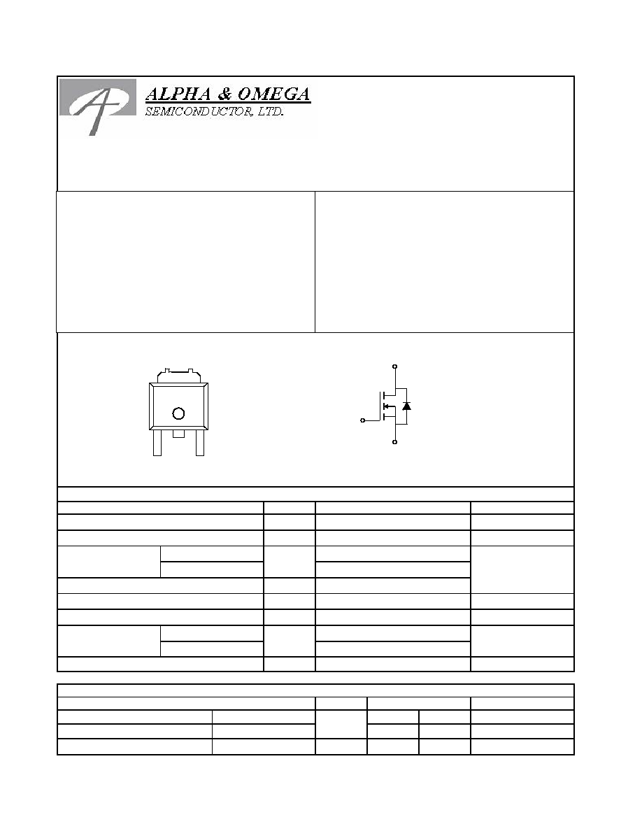
G
D
S
G D S
TO-252
D-PAK
Top View
Drain Connected to
Tab
Alpha & Omega Semiconductor, Ltd.

AOD442. AOD442L
Symbol
Min
Typ
Max
Units
BV
DSS
60
V
1
T
J
=55°C
5
I
GSS
100
nA
V
GS(th)
1
2.1
3
V
I
D(ON)
60
A
16
20
T
J
=125°C
31
20
25
m
g
FS
4.5
5.6
S
V
SD
0.74
1
V
I
S
4
A
C
iss
1920
2300
pF
C
oss
155
pF
C
rss
116
pF
R
g
0.65
0.8
Q
g
(10V)
47.6
68
nC
Q
g
(4.5V)
24.2
30
nC
Q
gs
6
nC
Q
gd
14.4
nC
t
D(on)
7.4
ns
t
r
5.1
ns
t
D(off)
28.2
ns
t
f
5.5
ns
t
rr
34
41
ns
Q
rr
46
nC
THIS PRODUCT HAS BEEN DESIGNED AND QUALIFIED FOR THE CONSUMER MARKET. APPLICATIONS OR USES AS CRITICAL
COMPONENTS IN LIFE SUPPORT DEVICES OR SYSTEMS ARE NOT AUTHORIZED. AOS DOES NOT ASSUME ANY LIABILITY ARISING
OUT OF SUCH APPLICATIONS OR USES OF ITS PRODUCTS. AOS RESERVES THE RIGHT TO IMPROVE PRODUCT DESIGN,
FUNCTIONS AND RELIABILITY WITHOUT NOTICE
Body Diode Reverse Recovery Time
Body Diode Reverse Recovery Charge I
F
=20A, dI/dt=100A/µs
Drain-Source Breakdown Voltage
On state drain current
I
D
=250µA, V
GS
=0V
V
GS
=10V, V
DS
=5V
V
GS
=10V, I
D
=20A
Reverse Transfer Capacitance
I
F
=20A, dI/dt=100A/µs
Electrical Characteristics (T
J
=25°C unless otherwise noted)
STATIC PARAMETERS
Parameter
Conditions
I
DSS
µ
A
Gate Threshold Voltage
V
DS
=V
GS
I
D
=250µA
V
DS
=48V, V
GS
=0V
V
DS
=0V, V
GS
= ±20V
Zero Gate Voltage Drain Current
Gate-Body leakage current
R
DS(ON)
Static Drain-Source On-Resistance
Forward Transconductance
Diode Forward Voltage
m
V
GS
=4.5V, I
D
=20A
I
S
=1A,V
GS
=0V
V
DS
=5V, I
D
=20A
Total Gate Charge
Gate Source Charge
Gate resistance
V
GS
=0V, V
DS
=0V, f=1MHz
Turn-On Rise Time
Turn-Off DelayTime
V
GS
=10V, V
DS
=30V, R
L
=1.5,
R
GEN
=3
Turn-Off Fall Time
Maximum Body-Diode Continuous Current
Input Capacitance
Output Capacitance
Turn-On DelayTime
DYNAMIC PARAMETERS
V
GS
=10V, V
DS
=30V, I
D
=20A
Total Gate Charge
Gate Drain Charge
V
GS
=0V, V
DS
=30V, f=1MHz
SWITCHING PARAMETERS
A: The value of R
JA
is measured with the device mounted on 1in
2
FR-4 board with 2oz. Copper, in a still air environment with T
A
=25°C. The Power
dissipation P
DSM
is based on R
JA
and the maximum allowed junction temperature of 150°C. The value in any a given application depends on the
user's specific board design, and the maximum temperature fo 175°C may be used if the PCB allows it.
B. The power dissipation P
D
is based on T
J(MAX)
=175°C, using junction-to-case thermal resistance, and is more useful in setting the upper dissipation
limit for cases where additional heatsinking is used.
C: Repetitive rating, pulse width limited by junction temperature T
J(MAX)
=175°C.
D. The R
JA
is the sum of the thermal impedence from junction to case R
JC
and case to ambient.
E. The static characteristics in Figures 1 to 6 are obtained using <300 µs pulses, duty cycle 0.5% max.
F. These curves are based on the junction-to-case thermal impedence which is measured with the device mounted to a large heatsink, assuming a
maximum junction temperature of T
J(MAX)
=175°C.
G. The maximum current rating is limited by bond-wires.
H. These tests are performed with the device mounted on 1 in 2 FR-4 board with 2oz. Copper, in a still air environment with T
A
=25°C. The SOA
curve provides a single pulse rating.
Alpha & Omega Semiconductor, Ltd.
AOD442. AOD442L
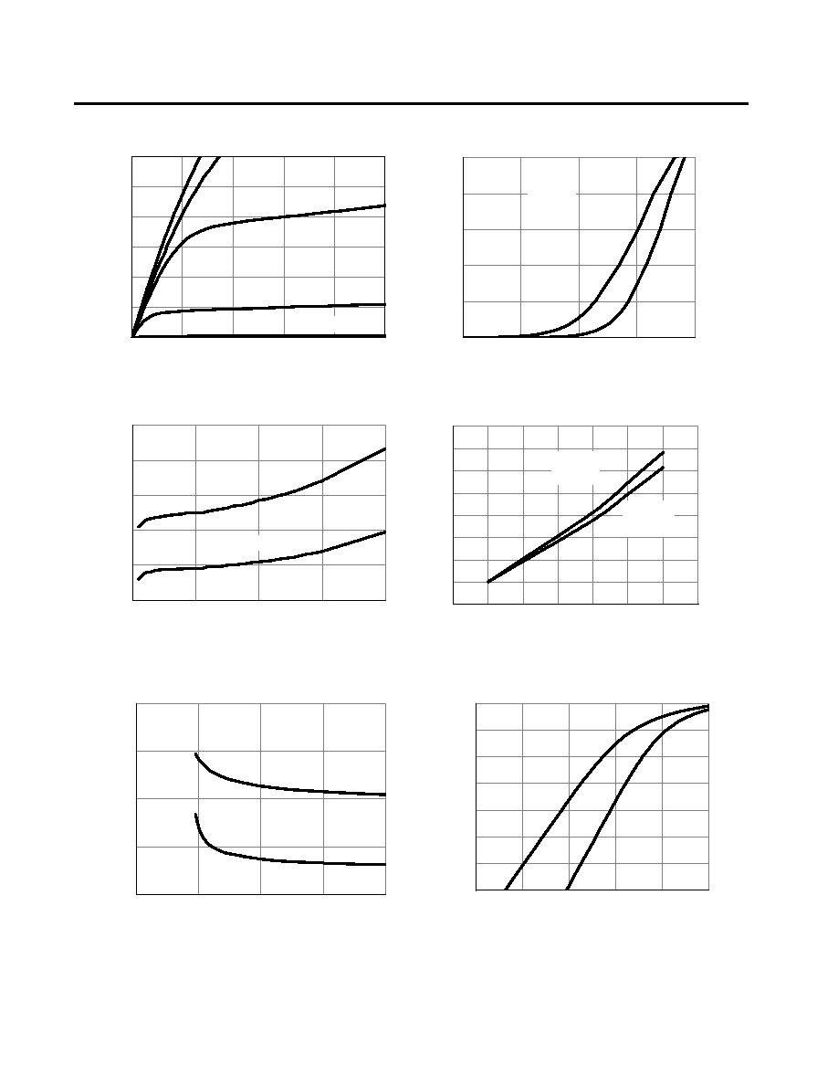
TYPICAL ELECTRICAL AND THERMAL CHARACTERISTICS
0
10
20
30
40
50
60
0
1
2
3
4
5
V
DS
(Volts)
Fig 1: On-Region Characteristics
I
D
(A
)
V
GS
=3V
3.5V
4V
4.5V
10V
0
10
20
30
40
50
2
2.5
3
3.5
4
V
GS
(Volts)
Figure 2: Transfer Characteristics
I
D
(A
)
14
16
18
20
22
24
0
10
20
30
40
I
D
(A)
Figure 3: On-Resistance vs. Drain Current and
Gate Voltage
R
DS
(
O
N)
(m
)
1.0E-05
1.0E-04
1.0E-03
1.0E-02
1.0E-01
1.0E+00
1.0E+01
1.0E+02
0.0
0.2
0.4
0.6
0.8
1.0
V
SD
(Volts)
Figure 6: Body-Diode Characteristics
I
S
(A
)
25°C
125°C
0.8
1
1.2
1.4
1.6
1.8
2
2.2
2.4
0
25
50
75
100
125
150
175
Temperature (°C)
Figure 4: On-Resistance vs. Junction
Temperature
N
o
r
m
a
lized
On
-
R
esist
a
n
c
e
V
GS
=10V
V
GS
=4.5V
I
D
=20A
I
D
=20A
10
20
30
40
50
2
4
6
8
10
V
GS
(Volts)
Figure 5: On-Resistance vs. Gate-Source Voltage
R
DS
(
O
N)
(m
)
25°C
125°C
V
DS
=5V
V
GS
=4.5V
V
GS
=10V
I
D
=20A
25°C
125°C
Alpha & Omega Semiconductor, Ltd.
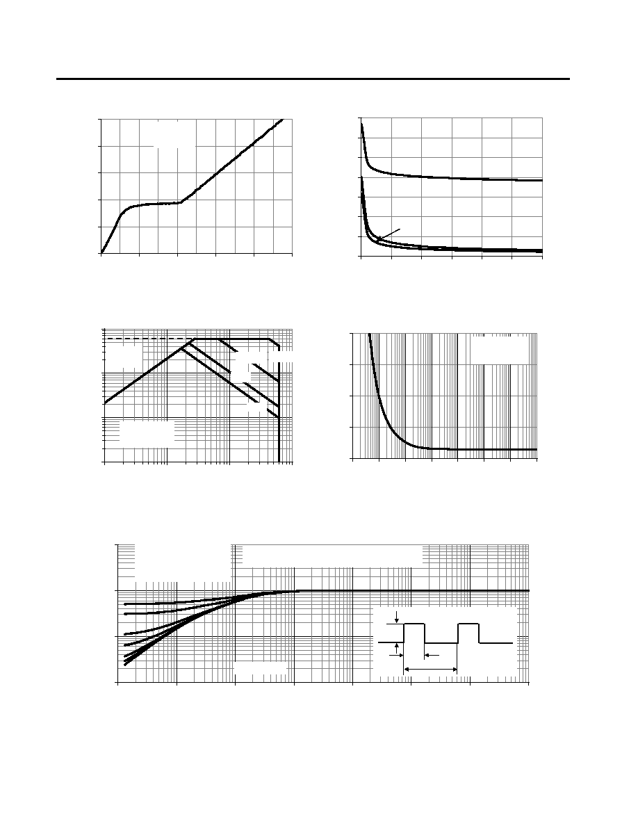
AOD442. AOD442L
TYPICAL ELECTRICAL AND THERMAL CHARACTERISTICS
0
2
4
6
8
10
0
10
20
30
40
50
Q
g
(nC)
Figure 7: Gate-Charge Characteristics
V
GS
(V
ol
ts)
0
500
1000
1500
2000
2500
3000
3500
0
5
10
15
20
25
30
V
DS
(Volts)
Figure 8: Capacitance Characteristics
C
a
pa
c
i
ta
nc
e
(pF)
C
iss
0
200
400
600
800
1E-05 1E-04 0.001 0.01
0.1
1
10
100
Pulse Width (s)
Figure 10: Single Pulse Power Rating Junction-to-
Case (Note F)
Po
w
e
r (
W
)
0.01
0.1
1
10
0.00001
0.0001
0.001
0.01
0.1
1
10
100
Pulse Width (s)
Figure 11: Normalized Maximum Transient Thermal Impedance (Note F)
Z
Jc
N
o
r
m
a
liz
ed
T
r
an
sien
t
T
h
er
m
al R
esistan
ce
C
oss
C
rss
0.1
1.0
10.0
100.0
0.1
1
10
100
V
DS
(Volts)
I
D
(A
m
p
s)
Figure 9: Maximum Forward Biased Safe
Operating Area (Note F)
100µs
1ms
DC
T
J(Max)
=175°C
T
A
=25°C
R
DS(ON)
limited
V
DS
=30V
I
D
=20A
Single Pulse
D=T
on
/T
T
J,PK
=T
c
+P
DM
.Z
Jc
.R
Jc
R
JC
=2.5°C/W
T
on
T
P
D
In descending order
D=0.5, 0.3, 0.1, 0.05, 0.02, 0.01, single pulse
T
J(Max)
=175°C
T
A
=25°C
10µs
Alpha & Omega Semiconductor, Ltd.
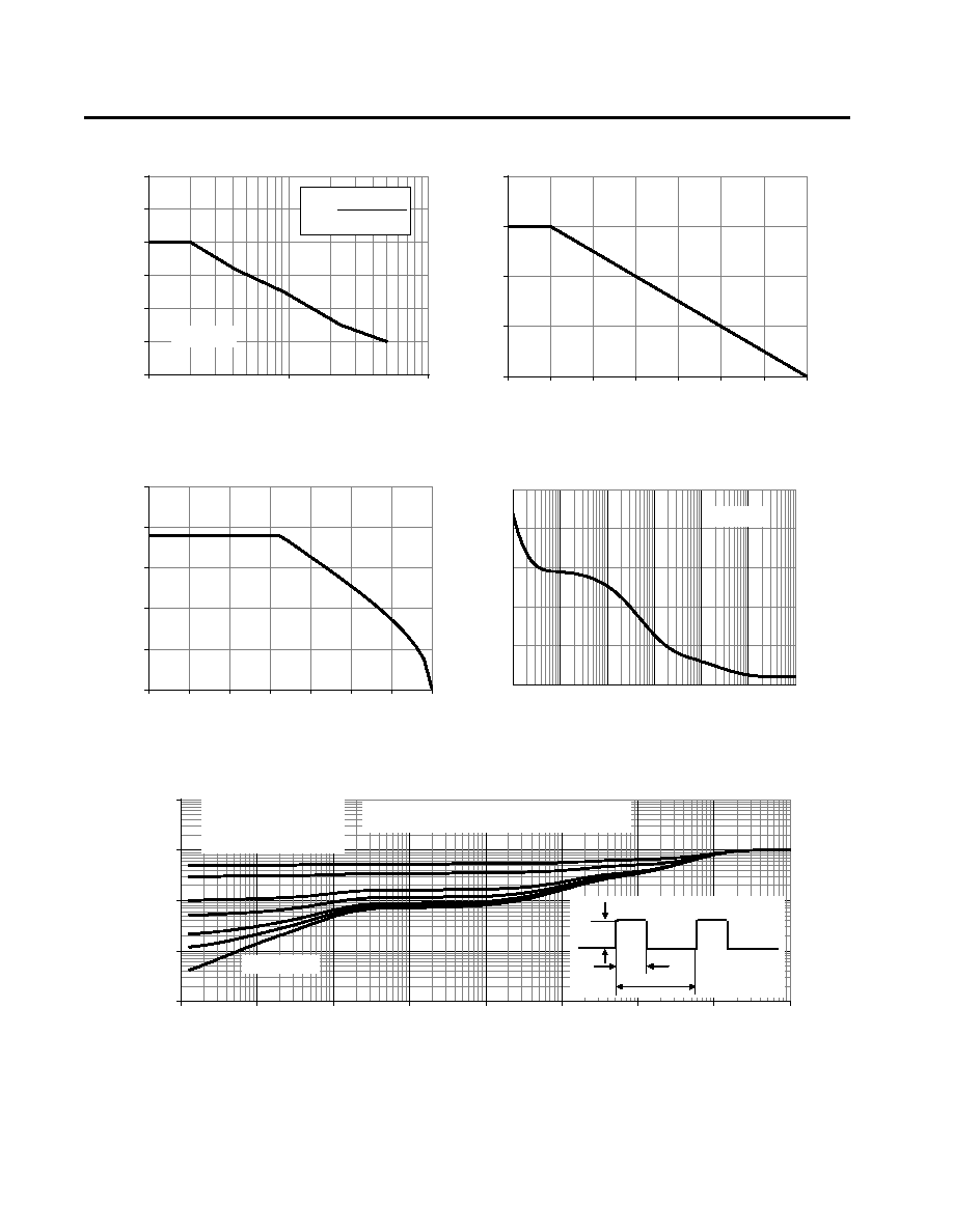
AOD442, AOD442L
TYPICAL ELECTRICAL AND THERMAL CHARACTERISTICS
0
10
20
30
40
50
60
0.00001
0.0001
0.001
Time in avalanche, t
A
(s)
Figure 12: Single Pulse Avalanche capability
I
D
(A
),
Peak A
val
an
ch
e C
u
r
r
en
t
0
20
40
60
80
0
25
50
75
100
125
150
175
T
CASE
(°C)
Figure 13: Power De-rating (Note B)
P
ow
e
r Dis
s
ipa
t
ion (
W
)
0
10
20
30
40
50
0
25
50
75
100
125
150
175
T
CASE
(°C)
Figure 14: Current De-rating (Note B)
Curre
nt
ra
t
ing I
D
(A
)
DD
D
A
V
BV
I
L
t
-
=
T
A
=25°C
0
10
20
30
40
50
0.001
0.01
0.1
1
10
100
1000
Pulse Width (s)
Figure 15: Single Pulse Power Rating Junction-to-
Ambient (Note H)
Po
wer
(W
)
T
A
=25°C
0.001
0.01
0.1
1
10
0.00001
0.0001
0.001
0.01
0.1
1
10
100
1000
Pulse Width (s)
Figure 16: Normalized Maximum Transient Thermal Impedance (Note H)
Z
JA
Norm
a
lize
d Tra
ns
ie
nt
T
h
er
mal
R
esi
stan
ce
Single Pulse
D=T
on
/T
T
J,PK
=T
A
+P
DM
.Z
JA
.R
JA
R
JA
=60°C/W
T
on
T
P
D
In descending order
D=0.5, 0.3, 0.1, 0.05, 0.02, 0.01, single pulse
Alpha & Omega Semiconductor, Ltd.
Document Outline
- aod442_rev2_green.pdf
- aod442_rev1_green.pdf
- aod442_rev1_green.pdf
- aod442_rev1_green.pdf
- aod442_rev1LFcover.pdf
- aod442_green_preliminary.pdf
- aod442_green_preliminary.pdf
- aod442_LFrev1.pdf
- aod442_LFrev1cover.pdf
- tape&reel.pdf
- aod436_rev1.pdf
- aod436_LF_Rev2_cover.pdf