 | –≠–ª–µ–∫—Ç—Ä–æ–Ω–Ω—ã–π –∫–æ–º–ø–æ–Ω–µ–Ω—Ç: AS2208 | –°–∫–∞—á–∞—Ç—å:  PDF PDF  ZIP ZIP |

ASTEC Semiconductor
Description
The AS2208 is a simplified pulse width modulation control-
ler, offering similar functionality as that of the AS3842.
Based on the AS2214, the AS2208 provides the additional
features of low startup current and overvoltage latching,
making it a good solution for adapter applications.
The PWM function is controlled by the current sense com-
parator for normal current mode control. The COMP pin,
which serves as an input to the current sense comparator,
provides a 1 mA current source which can be tied directly to
the control loop optocoupler. The output stage is a high
current totem pole output that sees only 85 ns delay from the
PWM comparator.
The AS2208 requires only 100
µ
A of startup current. The
undervoltage lockout (UVLO) thresholds are nominally 14V
for turn on and 8 V for turn off. The VREG pin, based on a
trimmed bandgap reference, provides a temperature com-
pensated 5 V to loads of up to 50 mA. The oscillator
discharge current is trimmed to provide guaranteed duty
cycle clamping.
AS2208
Primary Side PWM Controller
Preliminary Specification
Features
∑
Low Startup Current
∑
Single-start or auto-restart
modes
∑
Oscillator trimmed for precision
duty cycle clamp
∑
Standard temperature range
extended to 105
∞
C
∑
Remote on / off control
∑
Self limiting supply Voltage
∑
Standard current mode control
Pin Configuration
--
Top view
Ordering Information
Package Temperature Range Order Code
8-Pin Plastic DIP 0 to 105
∞
C AS2208N
8-Pin Plastic SOIC 0 to 105
∞
C AS2208D
77
8
1
7
2
GND
6
3
OV
VREG
5
4
RT/CT
OUT
COMP
VCC
ISNS
8L SOIC (D)
PDIP (N)
8
1
7
2
GND
6
3
OV
VREG
5
4
RT/CT
OUT
VCC
ISNS
COMP
AS2208
Primary Side PWM Controller
ASTEC Semiconductor
78
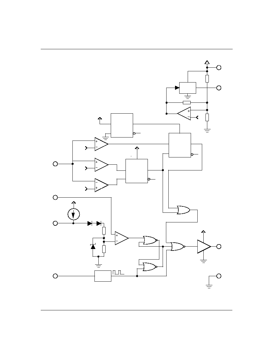
Functional Block Diagram
OV
UVLO
COMP
2R
R
ISNS
1V
OSC
RT/CT
CM PWM
OUT
GND
1V7
3V9
2V5
(BLANK)
5V enable
(PWM)
V
CC
V
REG
V
CC
5V Reg.
ENBL
S
Q
R
ENBL
S
Q
R
ENBL
S
Q
R
V
REG
V
REG
(FAULT)
Latch Enable
VOV Latch
Fault Latch
V
CC
1mA

Primary Side PWM Controller
AS2208
79
ASTEC Semiconductor
Pin Function Description
Pin Number
Function
Description
1
COMP
This is the inverting input to the PWM comparator. A divided and level shifted
representation of this voltage is compared to the ISNS input to determine OUT duty
cycle. A 1 mA current source is provided as a pull-up for an optocoupler.
2
ISNS
A voltage proportional to inductor current is connected to this pin. The PWM uses this
information to terminate the gate drive of the output.
3
RT/CT
Oscillator frequency and maximum duty cycle are set by connecting a resistor (R
T
) to
VREG and a capacitor (C
T
) to ground.
4
OV
This pin latches OUT low when pulled above 2.5 V. The latch can be reset by pulling
OV above 4 V then back to ground.
5
GND
Circuit common ground.
6
OUT
This totem pole output is designed to directly drive a power MOSFET switch capable of
sourcing and sinking peak currents up to 1 A.
7
V
CC
Positive supply voltage for the IC.
8
V
REG
Output of 5V series regulator.
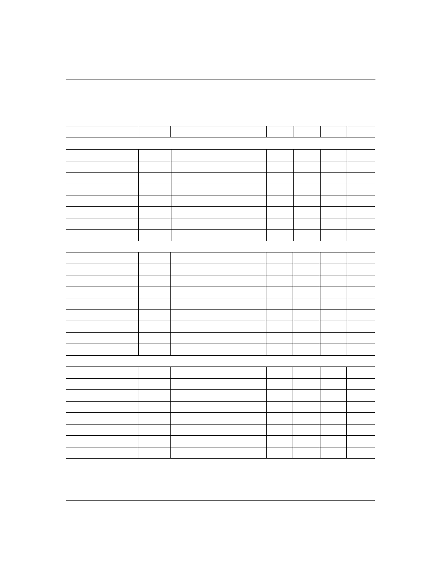
Absolute Maximum Ratings
Parameter
Symbol
Rating
Unit
Supply Voltage (I
CC
< 30 mA)
V
CC
Self-Limiting
V
Supply Voltage (Low Impedance Source)
V
CC
20
V
Reference Current
I
REF
200
mA
Output Current
I
OUT
1
A
Output Voltage
V
OUT
20
V
Continuous Power Dissipation at 25
∞
C
P
D
500
mW
Junction Temperature
T
J
150
∞
C
Storage Temperature Range
T
STG
≠ 65 to 150
∞
C
Lead Temperature, Soldering 10 Seconds
T
L
300
∞
C
Stresses greater than those listed under ABSOLUTE MAXIMUM RATINGS may cause permanent damage to the device. This is a stress
rating only and functional operation of the device at these or any other conditions above indicated in the operational sections of this
specification is not implied. Exposure to absolute maximum rating conditions for extended periods may affect reliability.
Recommended Conditions
Parameter Symbol Rating Unit
Supply Voltage
V
CC
10 - 15
V
Oscillator
F
OSC
50 - 250
kHz
Typical Thermal Resistance
Package
JA
JC
Typical Derating
8L PDIP 95
∞
C/W 50
∞
C/W
10.5 mW/
∞
C
8L SOIC 175
∞
C/W 45
∞
C/W
5.7 mW/
∞
C
AS2208
Primary Side PWM Controller
ASTEC Semiconductor
80
Electrical Characteristics
Electrical Characteristics are guaranteed over full junction temperature range (0 to 105
∞
C). Ambient temperature must be derated
based on power dissipation and package thermal characteristics. Unless otherwise specified, the conditions of test are V
CC
= 15 V;
BOK = 3 V; OV = 0V; R
T
= 680
; C
T
= 10 nF. To override UVLO, V
CC
should be raised above 18 V prior to test.
Parameter
Symbol
Test Condition
Min
Typ
Max
Unit
5 V Regulator
Output Voltage
V
REG
I
REG
= 1 mA, T
J
= 25
∞
C
4.90
5.00
5.10
V
Line Regulation
PSRR
9
V
CC
18 V
5
15
mV
Load Regulation
1
I
REG
20mA
5
15
mV
Temperature Stability
TC
REG
0.2
0.4
mV/
∞
C
Total Output Variation
Line, Load,Temperature
4.85
5.15
V
Long-Term Stability
Over 1,000 hrs at 25
∞
C
5
25
mV
Output Noise Voltage
V
NOISE
10
f
100kHz, T
J
= 25
∞
C
50
µ
V
Maximum Source Current
I
MAX
V
REG
= 4.8 V
30
120
180
mA
Oscillator
Initial Accuracy
F
OSC
T
J
=25
∞
C
108
120
132
kHz
Voltage Stability
9
V
CC
18 V
0.2
1
%
Temperature Stability
TC
F
T
MIN
T
J
T
MAX
5
%
Amplitude
V
OSC
V
RT/CT
peak-to-peak
1.55
V
Upper Trip Point
V
H
2.80
V
Lower Trip Point
V
L
1.25
V
Discharge Current
I
DSC
7.50
8.70
9.50
mA
Duty cycle Limit
R
T
=680
, C
T
=10nF, T
J
=25
∞
C
46
50
55
%
Over-Temperature Shutdown
T
OT
140
∞
C
Current Sense Comparator
Transfer Gain
AV
ISNS
-0.2
V
ISNS
0.8 V
2.85
3.00
3.15
V/V
ISNS Level Shift
V
LS
V
ISNS
= 0 V
1.50
V
Maximum Input Signal
V
ISNS MAX
V
COMP
=+5 V
1.00
1.08
1.20
V
Input Bias Current
I
BIAS ISNS
V
COMP
=+5 V
-1
-10
µ
A
COMP Source Current
I
COMPH
V
COMP
=+5 V
0.6
1.0
mA
COMP Swing High
V
COMPH
5.2
5.6
V
Power Supply Rejection Ratio
PSRR
9
V
CC
18 V
70
dB
Propagation Delay to Output
t
PB
85
150
ns

Primary Side PWM Controller
AS2208
81
ASTEC Semiconductor
Electrical Characteristics
(cont'd)
Electrical Characteristics are guaranteed over full junction temperature range (0 to 105
∞
C). Ambient temperature must be derated
based on power dissipation and package thermal characteristics. Unless otherwise specified, the conditions of test are V
CC
= 15 V;
BOK = 3 V; OV = 0V; R
T
= 680
; C
T
= 10 nF. To override UVLO, V
CC
should be raised above 18 V prior to test.
Parameter
Symbol
Test Condition
Min
Typ
Max
Unit
Output
Output Low Level
V
OL
I
SINK
= 20 mA
0.1
0.4
V
Output Low Level
V
OL
I
SINK
= 150 mA
1.5
2.2
V
Output High Level
V
OH
I
SOURCE
= 20 mA
13
13.5
V
Output High Level
V
OH
I
SOURCE
= 150 mA
12
13
V
Rise Time
t
R
C
L
= 1 nF
50
150
ns
Fall Time
t
F
C
L
= 1 nF
50
150
ns
Maximum Duty Cycle
D
MAX
94
97
100
%
Minimum Duty Cycle
D
MIN
0
%
Over-Voltage Input
OV Threshold
V
OV
2.50
2.80
3.10
V
OV Reset Threshold
V
VOVH
3.80
4.00
4.50
V
OV Clear Threshold
V
VOVL
1.10
1.75
2.20
V
OV Bias Current
I
BIAS OV
V
REG
= 5 V, V
OV
OV Threshold
-1
-0.2
1
µ
A
Under Voltage Lockout
Startup Threshold
V
CC
(ON)
12.5
14.0
15.8
V
Minimum Operating Voltage
V
CC
(OFF)
7.3
8.0
8.5
AV
after Turn-on
Startup Current
I
CC
V
CC
= 13 V
105
150
µ
A
Operating Supply Current
I
CC
12
20
mA
Supply Voltage Clamp
V
CC
Zener
I
CC
= 30 mA
18
V
Output Impedance to GND in
Z
OUT
V
CC
= 6 V
22.0
k
UVLO State
ASTEC reserves the right to make changes without further notice to any products described herein to improve reliability, function, or
design. ASTEC does not assume any liability arising out of the application or use of any product or circuit described herein; neither does
it convey any license under its patent rights or the rights of others. ASTEC products are not authorized for use as components in life
support devices or systems intended for surgical implant into the body or intended to support or sustain life. Buyer agrees to notify
ASTEC of any such intended end use whereupon ASTEC will determine availability and suitability of its products for the intended use.
ASTEC and the ASTEC logo are trademarks of ASTEC (BSR) PLC.
ASTEC SEMICONDUCTOR
255 Sinclair Frontage Road
∑
Milpitas, California 95035
∑
Tel. (408) 263-8300
∑
FAX (408) 263-8340