 | –≠–ª–µ–∫—Ç—Ä–æ–Ω–Ω—ã–π –∫–æ–º–ø–æ–Ω–µ–Ω—Ç: AT1008F | –°–∫–∞—á–∞—Ç—å:  PDF PDF  ZIP ZIP |

AT1008F
8-Channel ADPCM Processor
-
1
-
Copyright © 2000, Atelic Systems Inc.
Atelic Systems Inc.
AT1008F Application Note
8-Channel ADPCM Processor
Description
The AT1008F is an eight full-duplex channel ADPCM processor. It follows G.726 ITU Standard for ADPCM
compression for 40k, 32k, 24k and 16k with selectable
µ
-law and A-law input/output. This chip can operate on 16
channels of PCM to ADPCM compression, 16 channels of ADPCM to PCM decompression, 8 channels of full-
duplex operation in an 8KHz frame basis, or any combination of M-channels of compression plus N-channels of
decompression when M+N
16. Through its three wire serial port, the chip can be dynamically programmed to
perform the ADPCM algorithm at different bit rates, idle or reset of the algorithm. It can also be programmed to set
up different input/output time bit-slots, or to select, (1) bypass without compression at 64kbps PCM, (2) idle, or (3)
reset of the algorithm.
Features
∑
ADPCM coding and decoding with bypass mode
∑ µ
-law or A-law PCM selectable
∑
ITU-T G.726 compatible at 40kbps, 32kbps, 24kbps and 16kbps
∑
8 full duplex channels of operation, or any combination of (M encodes + N decodes) where M+N
16.
∑
Up to 8 synchronous signals for direct interface with popular combo/codec.
∑
Flexible on-chip time bit-slot assignment circuits.
∑
Internal clock generator and frame sync. generator
∑
The attributes for each individual channel such as compression rate, input/output time bit-slots, etc. can be
independently configured through the three wire serial port.
∑
On-chip power-on reset
∑
28-pin DIP or SOP packages
∑
The two clock pins (CLKA and CLKP) used as PCM/ADPCM data clocks and the two pins (FSX and FSY)
used for the two Frame Sync signals can be programmed to become either as input pins or as output pins. (The
defaults are as input pins).
Applications
∑
Wireless or wireline telephone systems
∑
PBX systems
∑
T1/E1applications
∑
Digital voice storage and recording devices

AT1008F
8-Channel ADPCM Processor
-
2
-
Copyright © 2000, Atelic Systems Inc.
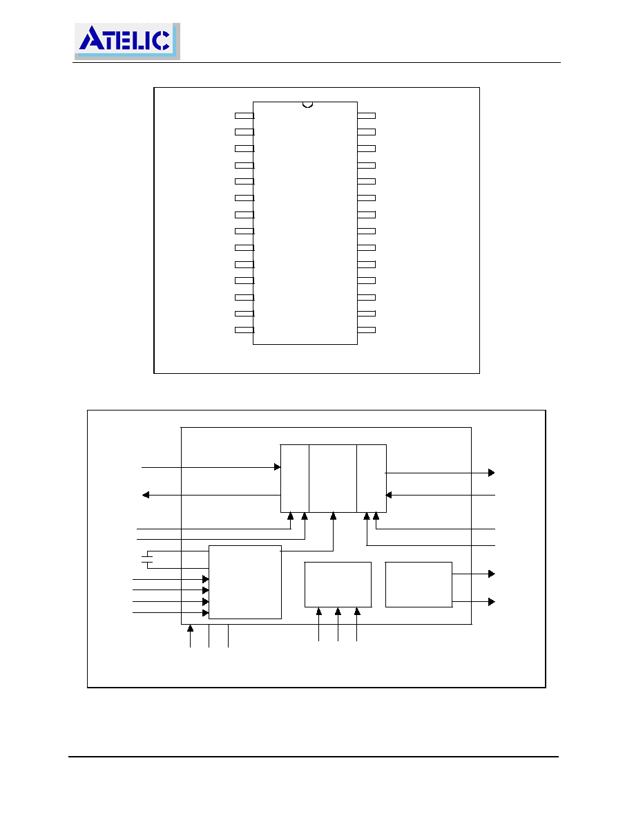
PIN Description
See figure 1 for PIN assignment.
PIN
SYMBOL
TYPE
DESCRIPTION
16
XIN
I
X Channel Data In. Sampled on the falling edge of CLKX during selected
time slots.
18
FSX/SYNC1
I/O
X Channel Frame Sync. Master X Channel Frame Sync. signal followed
by the first time slot of transmission. It can be either input or output by
initial setup sequence.
Sync 1. Frame sync. for 1
st
CODEC.
20
XOUT
O
X Channel Data Out. Updated on the rising edge of CLKX during
selected time slots.
27
YIN
I
Y Channel Data In. Sampled on the falling edge of CLKY during selected
time slots.
25
FSY
I/O
Y Channel Frame Sync. Master X Channel Frame Sync. signal followed
by the first time slot of transmission. It can be either input or output by
initial setup sequence.
24
YOUT
O
Y Channel Data Out. Updated on the rising edge of CLKY during
selected time slots.
2
RSTZ
I
Reset. Low active signal to force chip reset.
13
12
XTAL1/MCLK
XTAL2
I
O
Crystal In & Out. 10MHz source or 14.318 (10.000) MHz Crystal
connected.
17
CLKP
I/O
PCM Clock. It can be either input created by external control circuit, or
output generated by internal control circuit.
26
CLKA
I/O
ADPCM Clock. It can be either input created by external control circuit, or
output generated by internal control circuit.
15
11
10
9
8
5
1
SYNC2
SYNC3
SYNC4
SYNC5
SYNC6
SYNC7
SYNC8
O
O
O
O
O
O
O
Sync 2. Frame sync. for 2
nd
CODEC.
Sync 3. Frame sync. for 3
rd
CODEC.
Sync 4. Frame sync. for 4
th
CODEC.
Sync 5. Frame sync. for 5
th
CODEC.
Sync 6. Frame sync. for 6
th
CODEC.
Sync 7. Frame sync. for 7
th
CODEC.
Sync 8. Frame sync. for 8
th
CODEC.
4
3
TM1
TM0
I
I
TM1 & TM0 . Tie to Ground for normal operation.
7
6
A1
A0
I
I
A1 & A0. Address ID key for 3-wire serial port. If match, 3-wire serial port
can be enabled for configuration.
22
SDI
I
Serial Data In. Data for configuration on the fly by 3-wire serial port.
Sampled on the rising edge of SCLK with LSB first.
21
SCLK
I
Serial Clock. Used to write to the 3-wire serial port registers.
23
SCSZ
I
Serial Port Chip Select. Low active to enable 3-wire serial port.
28
VDD
-
Power. 3.3 Volts.
14
19
Vss1
Vss2
-
-
Ground. 0 Volt.
AT1008F
8-Channel ADPCM Processor
-
3
-
Copyright © 2000, Atelic Systems Inc.
SYNC8 1
28
RSTZ 2
27
TM0 3
26
TM1 4
25
SYNC7 5
24
A0 6
23
A1 7
22
SYNC6 8
21
SYNC5 9
20
SYNC4 10
19
SYNC3 11
18
XTAL2 12
17
XTAL1 13
16
VSS1 14
15
VDD
YIN
CKLA
FSY
YOUT
SCSZ
SDI
SCLK
XOUT
VSS2
FSX/SYNC1
CLKP
XIN
SYNC2
Figure 1. AT1008F pin assignment.
Xin
Yout
Fsx
CLKP(PCM)
Xtal
TM0
TM1
A0
A1
Clock
Control
RSTZ VDD VSS
3-wire generator
SCSZ SCLK SDI
PCM Full duplex ADPCM
I/O Quad I/O
Transcoder
Xout
Yin
Fsy
CLKA
(ADPCM)
SYNC 2
SYNC 8
Figure 2. AT1008F functional block diagram.
AT1008F
8-Channel ADPCM Processor
-
4
-
Copyright © 2000, Atelic Systems Inc.
Power consumption
The AT1008F is powered by a 3.3 V source and draws 60-70 mA at full operation and < 1 mA in powerdown
mode.
AT1008F chip initialization
There are two different classes of resets available on the AT1008F chip. For the default reset, hold the RSTZ pin
low for 50 ms, this reset will bring the chip to a functioning default state. In the default state, the following
parameters are set:
Pins FSX, FSY, CLKP, CLKA default as input pins (chip will receive these signals from external source).
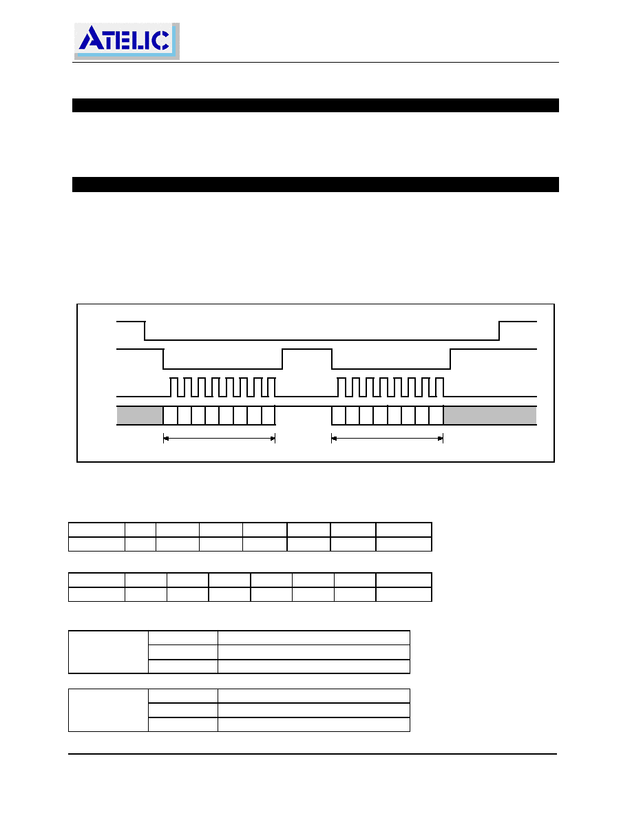
A second type of reset involving the use of the 3-wire serial interface can also be used direct the pin I/O
configurations of FSX, FSY, CLKP, and CLKA during reset.
SCLK
SCSZ
SDI
B0
B1
B5
B3
B4
B2
B6
B7
B0
B1
B3
B2
B4
B5
B7
B6
RSTZ
Byte 1
Byte 2
Figure 3. AT1008F FSX, FSY, CLKP, CLKA I/O direction configuration.
FSX, FSY, CLKP, CLKA I/O direction setup pattern (byte 1):
B7 (MSB)
B6
B5
B4
B3
B2
B1
B0 (LSB)
1
0
1
0
0
1
0
1
FSX, FSY, CLKP, CLKA I/O direction setup pattern (byte 2):
B7 (MSB)
B6
B5
B4
B3
B2
B1
B0 (LSB)
0
0
p5
p4
p3
P2
0
1
where:
value
description
0
CLKP set as output
p5
1
CLKP set as input
value
description
0
CLKA set as output
p4
1
CLKA set as input
AT1008F
8-Channel ADPCM Processor
-
5
-
Copyright © 2000, Atelic Systems Inc.
value
description
0
FSX set as output
p3
1
FSX set as input
value
description
0
FSY set as output
p2
1
FSY set as input
Configuration sequence: Write 2-bytes to the 3-wire serial interface when RSTZ is held active low. The first byte
written must be 0xA5 as a key to enter the AT1008F FSX, FSY, CLKP, CLKA I/O direction configuration mode; if
the first byte hasn't been written correctly, all four pins will remain set as input pins (default reset value).
Chip ID Setup
The two Chip ID pins A0 and A1 (Pins 6,7) should also be set during chip initialization. The "Chip ID" is used to
differentiate between AT1008F chips in a system that uses more than one AT1008F chip. When using only one
chip, it is recommended to tie A0 and A1 to digital zero. Thus, when programming the AT1008F chip, you can use
the Chip ID = `00' to substitute wherever you see A1, A0.