 | –≠–ª–µ–∫—Ç—Ä–æ–Ω–Ω—ã–π –∫–æ–º–ø–æ–Ω–µ–Ω—Ç: CX65003 | –°–∫–∞—á–∞—Ç—å:  PDF PDF  ZIP ZIP |
Skyworks Solutions, Inc. ∑ Phone [781] 376-3000 ∑ Fax [781] 376-3100 ∑ sales@skyworksinc.com ∑ www.skyworksinc.com
101468E ∑ Skyworks Proprietary and Confidential information ∑ Products and Product Information are Subject to Change Without Notice ∑ October 11, 2004
1
DATA SHEET
CX65003: 1400 ≠ 2500 MHz Linear Power Amplifier Driver
Applications
∑ PCS/DCS/2.5G/3G base stations
∑ Wireless Local Area Networks (WLANs)
∑ GSM/CDMA/W-CDMA handsets
∑ Wireless Local Loop (WLL) and Industrial, Scientific, Medical
(ISM) bands
∑ Repeaters
∑ Telematics
Features
∑ 5 V single supply operation
∑ Linear P
OUT
of 24.5 dBm
∑ OIP3 of 48 dBm
∑ Excellent W-CDMA performance
∑ Internal bias circuits
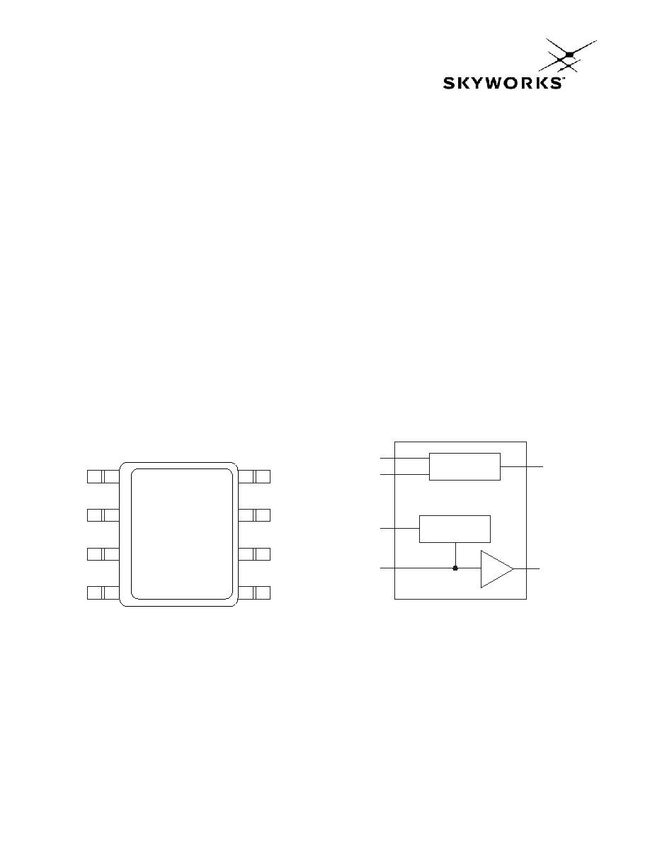
∑ 8-pin SOIC 5.994 x 4.928 mm package with downset paddle
1
2
3
4
8
7
6
5
C1215
NC
VB
RFIN
Y
VCC1
RFOUT
RFOUT
VCC2
Figure 1. CX65003 Pinout ≠ 8-Pin SOIC Package
(Top View)
Description
Skyworks CX65003 power amplifier driver offers a desirable
combination of features that provide superb performance and
ease of use in a low-cost Surface-Mounted Technology (SMT)
package. This Gallium Arsenide (GaAs) Heterojunction Bipolar
Transistor (HBT) power amplifier driver was developed and
optimized for extreme linear performance in a variety of
applications. It is ideal as a driver or output stage in transceivers
and repeaters for Wideband Code Division Multiple Access
(W-CDMA) and CDMA2000 applications.
The 8-pin Small Outline Integrated Circuit (SOIC) device package
and pinout are shown in Figure 1. Figure 2 shows a functional
block diagram for the CX65003. Signal pin assignments and
functional pin descriptions are provided in Table 1.
Driver Bias
Input Bias
VCC1
8
5
2
3
6
7
4
Y
VCC2
VB
RFIN
RFOUT
PA
C1216
Figure 2. CX65003 Functional Block Diagram
DATA SHEET ∑ CX65003
Skyworks Solutions, Inc. ∑ Phone [781] 376-3000 ∑ Fax [781] 376-3100 ∑ sales@skyworksinc.com ∑ www.skyworksinc.com
2
October 11, 2004 ∑ Skyworks Proprietary and Confidential information ∑ Products and Product Information are Subject to Change Without Notice ∑ 101468E
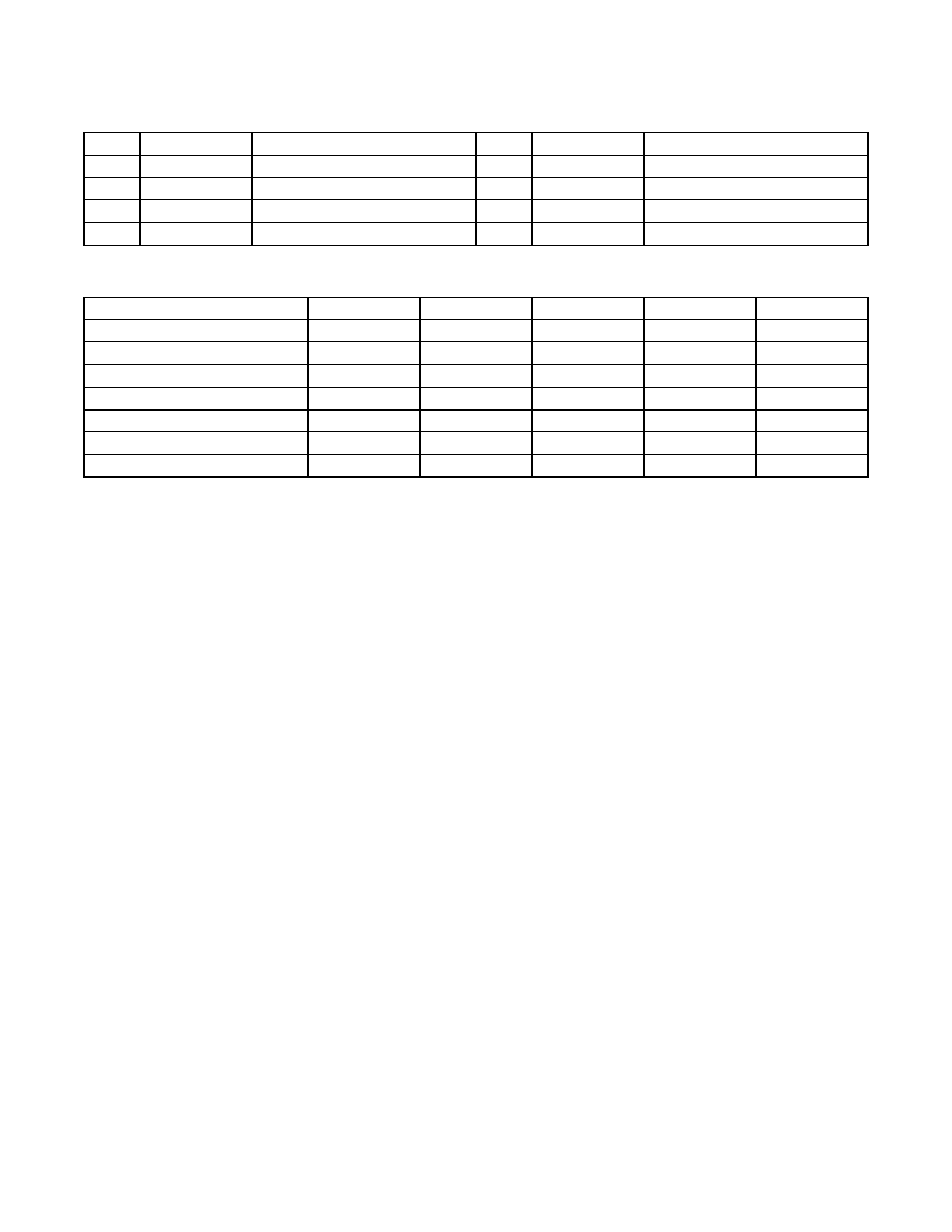
Table 1. CX65003 Signal Descriptions
Pin #
Name
Description
Pin #
Name
Description
1 NC
No
connection
5 VCC2
Supply
voltage
2
VB
Input bias for amplifier driver
6
RFOUT
RF output
3 RFIN
RF
input
7 RFOUT
RF
output
4
Y
Output of internal bias circuit
8
VCC1
Supply voltage
Table 2. CX65003 Absolute Maximum Ratings
Parameter Symbol
Min
Typical
Max
Units
RF input power
P
IN
15
dBm
Supply voltage (VCC1 and VCC2 pins)
VCC
5.5
V
Supply current (I
D
+ I
BIAS
) I
CC
240
mA
Power dissipation
1.3
W
Case operating temperature
T
C
≠40
+85
∞C
Storage temperature
T
ST
≠55
+125
∞C
Junction temperature
T
J
+150
∞C
Note: Exposure to maximum rating conditions for extended periods may reduce device reliability. There is no damage to device with only one parameter set at the limit and all other
parameters set at or below their nominal value.
Technical Description
The CX65003 is a single stage linear amplifier. The device can be
externally matched for optimum gain and linearity using two to
three passive components. These external components allow the
amplifier to be set to a desired operating frequency.
The CX65003 contains a bias circuit for optimum temperature
tracking performance. An external resistor is used to set the bias
current level. The value of this resistor can be selected to set the
amplifier operational mode to Class A, B, or AB.
Package and Handling Information
Since the device package is sensitive to moisture absorption, it is
baked and vacuum packed before shipping. Instructions on the
shipping container label regarding exposure to moisture after the
container seal is broken must be followed. Otherwise, problems
related to moisture absorption may occur when the part is
subjected to high temperature during solder assembly.
If the part is attached in a reflow oven, the temperature ramp rate
should not exceed 5
∞C per second. Maximum temperature
should not exceed 225
∞C and the time spent at a temperature
that exceeds 210
∞C should be limited to less than 10 seconds. If
the part is manually attached, precaution should be taken to
ensure that the part is not subjected to a temperature that
exceeds 300
∞C for more than 10 seconds.
Care must be taken when attaching this product, whether it is
done manually or in a production solder reflow environment.
Production quantities of this product are shipped in a standard
tape and reel format. For packaging details, refer to the Skyworks
Application Note, Tape and Reel, document number 101568.
Electrical and Mechanical Specifications
The absolute maximum ratings of the CX65003 are provided in
Table 2. The recommended operating conditions are specified in
Table 3 and electrical specifications are provided in Table 4.
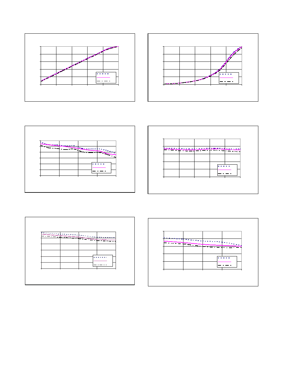
Typical performance characteristics of the CX65003 are shown in
Figures 3 through 18. Figure 25 provides the package dimensions
for the 8-pin SOIC and Figure 26 provides the tape and reel
dimensions.
Electrostatic Discharge (ESD) Sensitivity
The CX65003 is a static-sensitive electronic device. Do not
operate or store near strong electrostatic fields. Take proper ESD
precautions.

DATA SHEET ∑ CX65003
Skyworks Solutions, Inc. ∑ Phone [781] 376-3000 ∑ Fax [781] 376-3100 ∑ sales@skyworksinc.com ∑ www.skyworksinc.com
101468E ∑ Skyworks Proprietary and Confidential information ∑ Products and Product Information are Subject to Change Without Notice ∑ October 11, 2004
3
Table 3. CX65003 Recommended Operating Conditions
Parameter Symbol
Min
Typical
Max
Units
Supply voltage (VCC1 and VCC2 pins)
VCC
5
V
Operating frequency
F
O
1400 2500
MHz
Junction temperature
T
J
140
∞C
Maximum bias condition
(VCC
◊ I
D
) < (T
J
_
RECOMMENDED
≠ T
C
)/R
TH
,
J
-
C
Table 4. CX65003 Electrical Characteristics
(VCC = 5 V, T
C
= 25 ∞C)
Parameter Symbol
Test
Conditions Min
Typical
Max Units
OIP3 Match, Frequency = 1960 MHz (Note 1)
Quiescent current (l
D
+ l
BIAS
) Iq
R
BIAS
= 270
120
130
mA
Small signal gain
G
P
IN
= ≠15 dBm
10
11.5
dB
Linear output power (Note 2)
P
OUT
P
IN
= +13 dBm
23
24.5
dBm
Power Added Efficiency
PAE
P
IN
= +13 dBm
30
38
%
Noise Figure (NF)
NF
5
6
dB
Output IP3
OIP3
Two CW tones with 1 MHz
spacing, P
IN
= ≠4 dBm per
tone
42 48 dBm
Thermal resistance (junction ≠ case)
R
TH
,
J
-
C
65
∞C/W
ACPR Match, Frequency = 2140 MHz (Note 3)
Quiescent current (l
D
+ l
BIAS
) Iq
R
BIAS
= 330
90
105
mA
Small signal gain (Note 4)
G
P
IN
= ≠15 dBm
9.5
11
dB
Peak envelope power (Note 2)
P
PEP
3G-WCDMA downlink test
model #1 signal or IS95
downlink 9 ch Fwd signal,
P
IN
= 9 dBm
29 dBm
Average output power (F = 1.96 GHz)
@ ACPR = ≠45 dBc (Note 3), 885 kHz offset
P
OUT
ACPR
IS95 downlink CDMA
signal, 9 ch Fwd,
P
IN
= 11 dBm
20 21 dBm
Average output power (F = 2.14 GHz)
@ ACLR = ≠45 dBc, 5 MHz offset
P
OUT
ACLR
3G-WCDMA downlink test
model #1 signal with
64 DPCH, P
IN
= 9 dBm
18.5 20 dBm
Note 1: Device matched for optimum OIP3 according to circuit shown in Figure 21.
Note 2: For reliable operation, do not violate the maximum input drive level specified in Table 2.
Note 3: Device matched for optimum ACPR according to circuit shown in Figure 22.
Note 4: For optimum output small signal gain and Noise Figure, use the matching circuit shown in Figure 21 and the characterization values for 1960 MHz operation.
DATA SHEET ∑ CX65003
Skyworks Solutions, Inc. ∑ Phone [781] 376-3000 ∑ Fax [781] 376-3100 ∑ sales@skyworksinc.com ∑ www.skyworksinc.com
4
October 11, 2004 ∑ Skyworks Proprietary and Confidential information ∑ Products and Product Information are Subject to Change Without Notice ∑ 101468E
5
9
13
17
21
25
-5
-1
3
7
11
15
Pin (dBm)
P
out (dB
m
)
-40C
25C
85C
Figure 3. Typical P
OUT
vs P
IN
@ 1960 MHz Over Temperature
(Circuit Match for Optimum OIP3)
9
10
11
12
13
14
15
1400.0
1512.5
1625.0
1737.5
1850.0
Freq (MHz)
Small Signal Gain (
d
B)
-40C
25C
85C
Figure 5. Typical Small Signal Gain From 1.4 to 1.85 GHz Over
Temperature (Circuit Match for Optimum Gain)
7
8
9
10
11
12
13
2000
2050
2100
2150
2200
Freq (MHz)
Small Signal Gain (dB)
≠40C
25C
85C
Figure 7. Typical Small Signal Gain From 2 to 2.2 GHz Over
Temperature (Circuit Match for Optimum OIP3)
0
10
20
30
40
50
-5
-1
3
7
11
15
Pin (dBm)
PAE (
%
)
-40C
25C
85C
Figure 4. Typical PAE vs P
IN
@ 1960 MHz Over Temperature
(Circuit Match for Optimum OIP3)
8
9
10
11
12
13
1850
1880
1910
1940
1970
2000
Freq (MHz)
Small Signal Gain (dB)
-40C
25C
85C
Figure 6. Typical Small Signal Gain From 1.85 to 2.0 GHz Over
Temperature (Circuit Match for Optimum OIP3)
7
8
9
10
11
12
2300
2350
2400
2450
2500
Freq (MHz)
Small Signal Gain (dB)
-40C
25C
85C
Figure 8. Typical Small Signal Gain From 2.3 to 2.5 GHz Over
Temperature (Circuit Match for Optimum OIP3)

DATA SHEET ∑ CX65003
Skyworks Solutions, Inc. ∑ Phone [781] 376-3000 ∑ Fax [781] 376-3100 ∑ sales@skyworksinc.com ∑ www.skyworksinc.com
101468E ∑ Skyworks Proprietary and Confidential information ∑ Products and Product Information are Subject to Change Without Notice ∑ October 11, 2004
5
0
1
2
3
4
5
6
1400.0
1512.5
1625.0
1737.5
1850.0
Freq (MHz)
NF
(d
B)
-40C
25C
85C
Figure 9. Typical Noise Figure From 1.4 to 1.85 GHz Over
Temperature (Circuit Match for Optimum Gain)
0
1
2
3
4
5
6
2000
2050
2100
2150
2200
Freq (MHz)
NF
(d
B)
-40C
25C
85C
Figure 11. Typical Noise Figure From 2.0 to 2.2 GHz Over
Temperature (Circuit Match for Optimum OIP3)
30
35
40
45
50
55
1850
1880
1910
1940
1970
2000
Freq (MHz)
OIP3 (
d
Bm)
-40C
25C
85C
Figure 13. Typical OIP3 From 1.85 to 2.0 GHz Over Temperature
(Circuit Match for Optimum OIP3)
0
1
2
3
4
5
6
1850
1880
1910
1940
1970
2000
Freq (MHz)
NF
(d
B)
-40C
25C
85C
Figure 10. Typical Noise Figure From 1.85 to 2.0 GHz Over
Temperature (Circuit Match for Optimum OIP3)
0
1
2
3
4
5
6
7
8
2300
2350
2400
2450
2500
Freq (MHz)
NF
(d
B)
-40C
25C
85C
Figure 12. Typical Noise Figure From 2.3 to 2.5 GHz Over
Temperature (Circuit Match for Optimum OIP3)
30
35
40
45
50
2000
2050
2100
2150
2200
Freq (MHz)
OIP3 (dBm)
-40C
25C
85C
Figure 14. Typical OIP3 From 2.0 to 2.2 GHz Over Temperature
(Circuit Match for Optimum OIP3)