 | ÐлекÑÑоннÑй компоненÑ: CX65104 | СкаÑаÑÑ:  PDF PDF  ZIP ZIP |
Äîêóìåíòàöèÿ è îïèñàíèÿ www.docs.chipfind.ru
Skyworks Solutions, Inc. · Phone [781] 376-3000 · Fax [781] 376-3100 · sales@skyworksinc.com · www.skyworksinc.com
101475F · Skyworks Proprietary and Confidential Information · Products and Product Information are Subject to Change Without Notice · July 15, 2004
1
DATA SHEET
CX65104: 700 1000 MHz Linear Power Amplifier
Applications
· AMPS/CDMA/TDMA/GSM
· Repeaters
· WLL and ISM bands
· Mobile radio
· Paging
· Telematics
Features
· Typical P
OUT
of 31 dBm
· High linearity
· Low power consumption
· Single +5 V supply
· 8-pin LCC 8 x 8 mm package
Description
Skyworks CX65104 Power Amplifier (PA) is a fully matched, 8-pin
Leadless Chip Carrier (LCC) surface mount module, developed for
cellular, Wireless Local Loop (WLL), and Industrial, Scientific,
Medical (ISM) applications. This small, power-efficient PA has a
full 700 to 1000 MHz bandwidth coverage packed into a single
compact package.
All active circuitry in the module is contained in a single Gallium
Arsenide (GaAs) Microwave Monolithic Integrated Circuit (MMIC).
The CX65104 is manufactured with Skyworks Aluminum (Al) GaAs
Heterojunction Bipolar Transistor (HBT) process, which allows for
single supply operation while maintaining high efficiency and
good linearity.
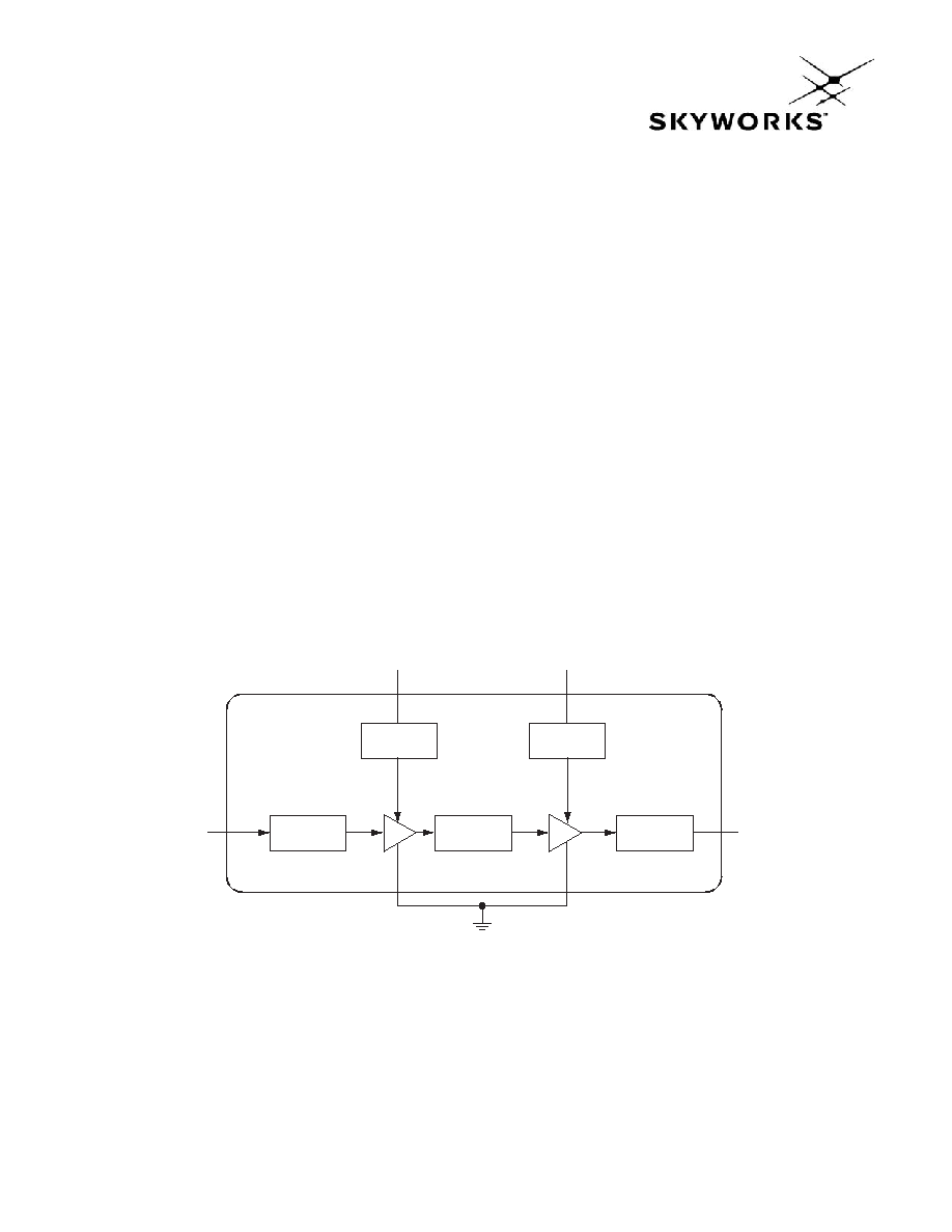
Figure 1 shows a functional block diagram for the CX65104. The
device package and pinout are shown in Figure 2. Signal pin
assignments and functional pin descriptions are provided in
Table 1.
Driver Amp
Bias
Input Match
PA
PA
RFIN
VCC1
2
RFOUT
6
8
1, 3, 5, 7
Power Amp
Bias
Interstage Match
Output Match
C1220a
VCC2
GND
4
Figure 1. CX65104 Functional Block Diagram
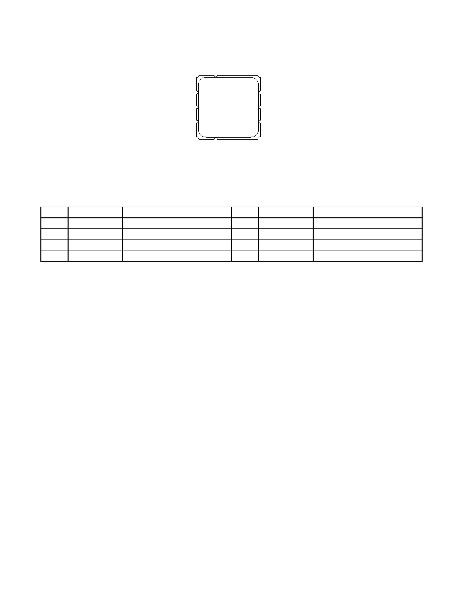
DATA SHEET · CX65104
Skyworks Solutions, Inc. · Phone [781] 376-3000 · Fax [781] 376-3100 · sales@skyworksinc.com · www.skyworksinc.com
2
July 15, 2004 · Skyworks Proprietary and Confidential Information · Products and Product Information are Subject to Change Without Notice · 101475F
1
2
3
4
GND
RFIN
GND
GND
RFOUT
GND
VCC1
VCC2
8
7
6
5
S385
Figure 2. CX65104 Pinout 8-Pin LCC Package
(Top View)
Table 1. CX65104 Signal Descriptions
Pin #
Name
Description
Pin #
Name
Description
1 GND
Ground
5 GND
Ground
2 RFIN
RF
input
6 RFOUT
RF
output
3 GND
Ground
7 GND
Ground
4 VCC2
Supply
voltage
8 VCC1
Supply
voltage
Technical Description
The CX65104 is comprised of two amplifier stages. The matching
circuits for the input stage, inter-stage, and output stage are
contained within the device. The bias circuits for both input and
output stages are included within the device for optimum
temperature tracking performance.
The CX65104 is internally matched for optimum linearity and
efficiency. The input and output stages are independently
supplied using the VCC1 and VCC2 supply lines, pins 8 and 4
respectively.
Package and Handling Information
Since the device package is sensitive to moisture absorption, it is
baked and vacuum packed before shipping. Instructions on the
shipping container label regarding exposure to moisture after the
container seal is broken must be followed. Otherwise, problems
related to moisture absorption may occur when the part is
subjected to high temperature during solder assembly.
If the part is attached in a reflow oven, the temperature ramp rate
should not exceed 5
°C per second. Maximum temperature
should not exceed 225
°C and the time spent at a temperature
that exceeds 210
°C should be limited to less than 10 seconds. If
the part is manually attached, precaution should be taken to
ensure that the part is not subjected to a temperature that
exceeds 300
°C for more than 10 seconds.
Care must be taken when attaching this product, whether it is
done manually or in a production solder reflow environment.
Production quantities of this product are shipped in a standard
tape and reel format. For packaging details, refer to the Skyworks
Application Note, Tape and Reel, document number 101568.
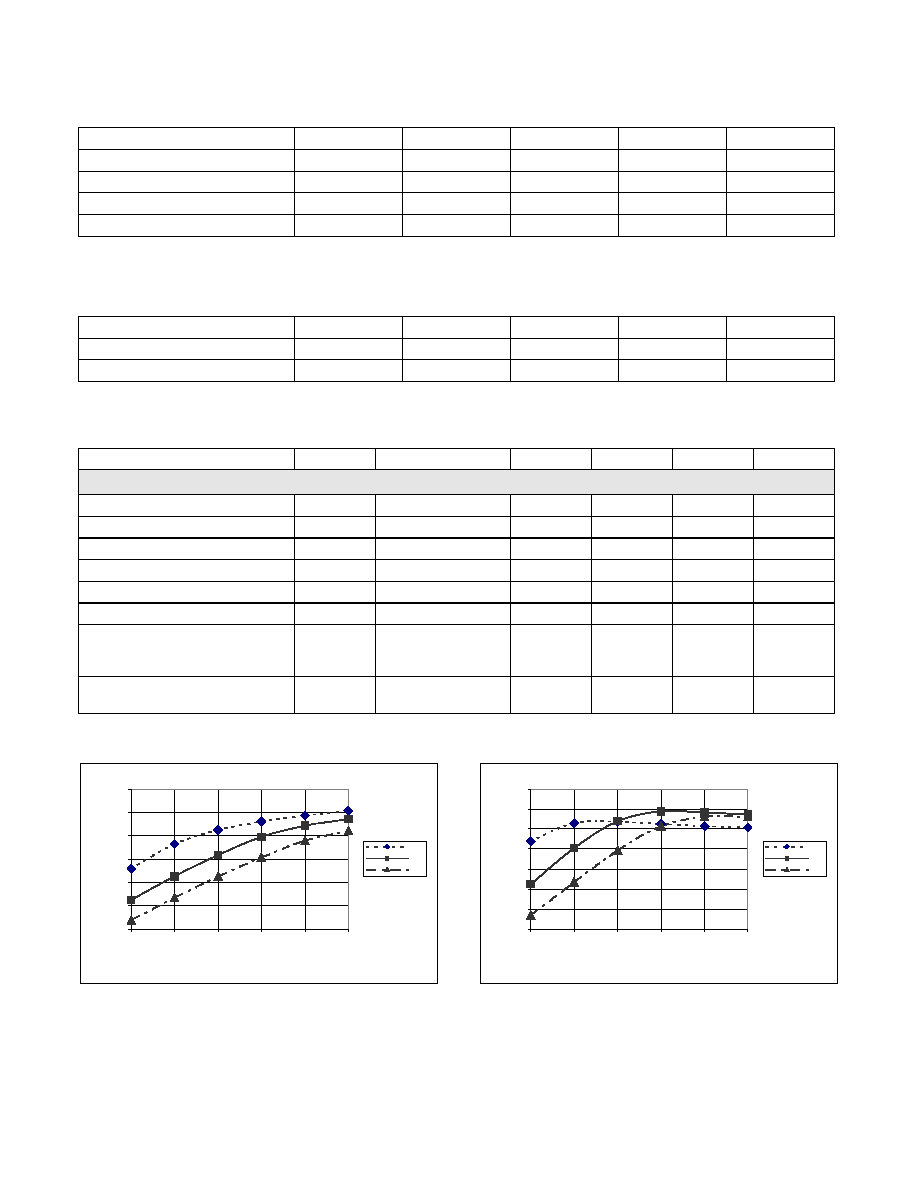
Electrical and Mechanical Specifications
The absolute maximum ratings of the CX65104 are provided in
Table 2. The recommended operating conditions are specified in
Table 3 and electrical specifications are provided in Table 4.
Typical performance characteristics over temperature of the
CX65104 are illustrated in Figures 3 through 8.
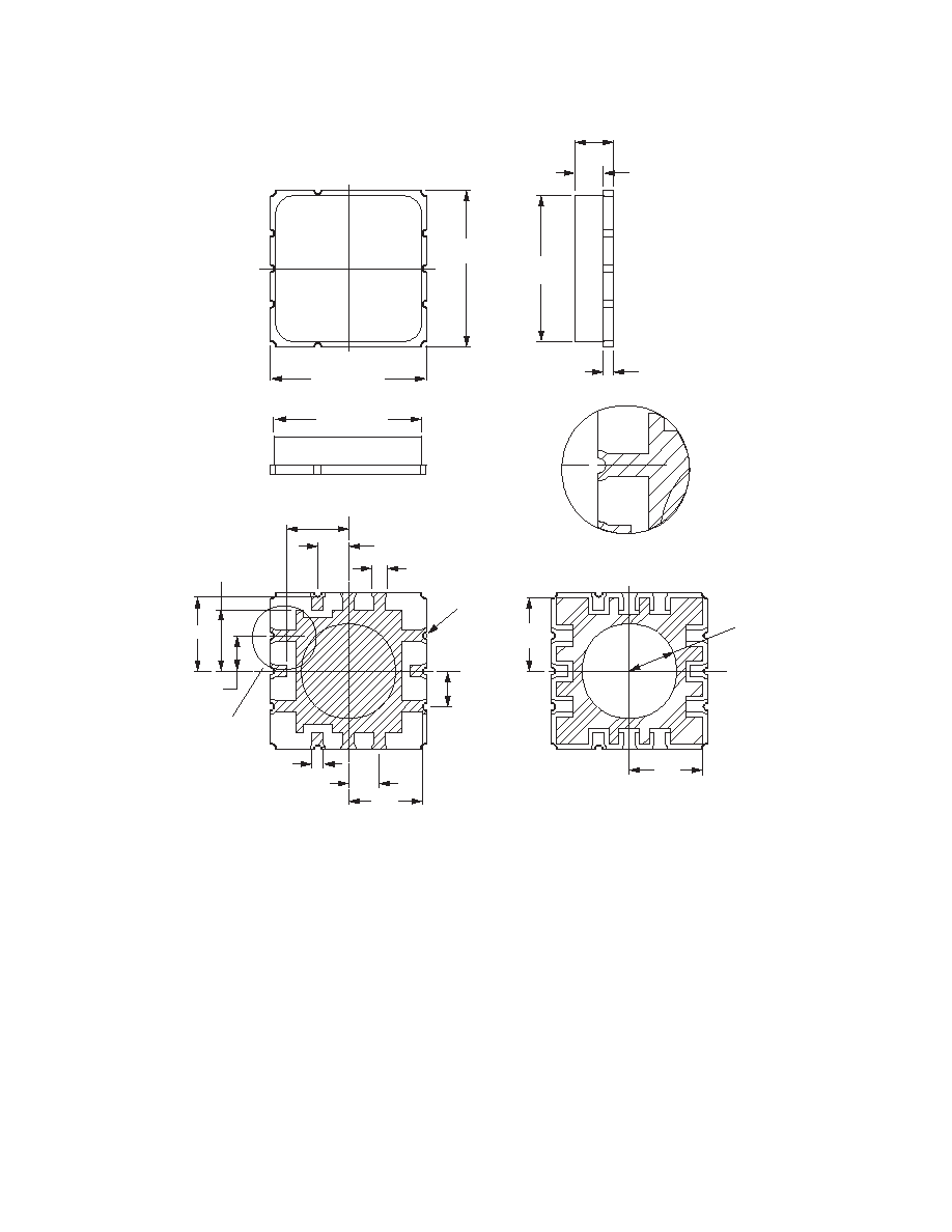
Figure 9 shows the package dimensions for the 8-pin CX65104
LCC and Figure 10 provides the tape and reel dimensions.
Electrostatic Discharge (ESD) Sensitivity
The CX65104 is a static-sensitive electronic device. Do not
operate or store near strong electrostatic fields. Take proper ESD
precautions.
DATA SHEET · CX65104
Skyworks Solutions, Inc. · Phone [781] 376-3000 · Fax [781] 376-3100 · sales@skyworksinc.com · www.skyworksinc.com
101475F · Skyworks Proprietary and Confidential Information · Products and Product Information are Subject to Change Without Notice · July 15, 2004
3
Table 2. CX65104 Absolute Maximum Ratings
Parameter Symbol
Min
Typical
Max
Units
RF input power
P
IN
10
dBm
Supply voltage
V
CC
8.5
V
Case operating temperature
T
C
40
+85
°C
Storage temperature
T
ST
55
+125
°C
Note: Exposure to maximum rating conditions for extended periods may reduce device reliability. There is no damage to device with only one parameter set at the limit and all other
parameters set at or below their nominal values.
Table 3. CX65104 Recommended Operating Conditions
Parameter Symbol
Min
Typical
Max
Units
Supply
voltage
VCC
5 V
Operating frequency
F
O
700
900
1000
MHz
Table 4. CX65104 Electrical Characteristics
(VCC = 5.0 V, Frequency = 900 MHz, T
C
= 25 °C, unless otherwise noted)
Parameter Symbol
Test
Conditions Min
Typical
Max Units
Analog Inputs
Frequency range
700
900
1000
MHz
Quiescent current
I
Q
75
100
mA
Small signal gain
G
P
IN
= 15 dBm
27
29
dB
Output power
P
OUT
P
IN
= 3 dBm
29.5
31.0
dBm
Efficiency PAE
P
IN
= 3 dBm
35
39
%
Noise Figure (NF)
NF
4
5
dB
Output IP3
OIP3
Two tones with 100 kHz
spacing, P
IN
= 5 dBm per
tone
37 42 dBm
P
OUT
@ ACPR = 45 dBc
P
OUT
_
ACPR
f = 881.5 MHz,
750 kHz offset
23 25 dBm
Note: The above specifications apply only to the 900 MHz operating frequency.
27
28
29
30
31
32
33
0
1
2
3
4
5
Pin (dBm)
Pout (dBm)
-30C
25C
85C
Figure 3. Typical P
OUT
vs P
IN
Over Temperature
27
29
31
33
35
37
39
41
0
1
2
3
4
5
Pin (dBm)
PA
E (
%
)
-30C
25C
85C
Figure 4. Typical PAE vs P
IN
Over Temperature
DATA SHEET · CX65104
Skyworks Solutions, Inc. · Phone [781] 376-3000 · Fax [781] 376-3100 · sales@skyworksinc.com · www.skyworksinc.com
4
July 15, 2004 · Skyworks Proprietary and Confidential Information · Products and Product Information are Subject to Change Without Notice · 101475F
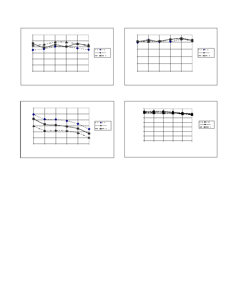
0
1
2
3
4
5
6
750
800
850
900
950
1000
Freq (MHz)
NF (dB)
-30C
25C
85C
Figure 5. Typical Noise Figure vs Frequency Over Temperature
25
26
27
28
29
30
31
750
800
850
900
950
1000
Freq (MHz)
Small Signal Gain (
d
B)
-30C
25C
85C
Figure 7. Typical Small Signal Gain vs Frequency Over
Temperature
0
10
20
30
40
50
750
800
850
900
950
1000
Freq (MHz)
OIP3 (
d
Bm)
-30C
25C
85C
Figure 6. Typical OIP3 vs Frequency Over Temperature
0.00
5.00
10.00
15.00
20.00
25.00
30.00
35.00
750
800
850
900
950 1000
Freq (MHz)
Pout (dBm)
-30C
25C
85C
Figure 8. Typical P
OUT
vs Frequency Over Temperature
DATA SHEET · CX65104
Skyworks Solutions, Inc. · Phone [781] 376-3000 · Fax [781] 376-3100 · sales@skyworksinc.com · www.skyworksinc.com
101475F · Skyworks Proprietary and Confidential Information · Products and Product Information are Subject to Change Without Notice · July 15, 2004
5
SOLDER MASK BOTTOM
COPPER BOTTOM
R.20 (8X)
7.875 ± 0.075
7.875 ± 0.075
1.91 (2X)
1.91 (2X)
0.61 (12X)
0.81 (12X)
R 2.54
The bottom solder mask thickness = 0.063 maximum
All measurements are in millimeters
3.94
3.94
1.65 (2X)
3.99
3.99
3.30 (2X)
1.65 (2X)
3.30 (2X)
1.45 ± 0.10
1.955 ± 0.155
0.51 ± 0.05
8.385 ± 0.125
8.385 ± 0.125
Pin 1
Pin 2
Pin 3
Pin 7
Pin 8
Pin 6
Pin 5
Pin 4
DETAIL A
SEE DETAIL A
Note: pin 1 connects to ground
Pin 9
C1201
Figure 9. CX65104 8-Pin LCC Package Dimensions