
MDT2051
This specification are subject to be changed without notice. Any latest information please preview
http;//www.mdtic.com.tw
P. 1
2004/1 Ver. 1.8
1. General Description
This EPROM-Based 8-bit micro-controller uses a fully
static CMOS technology process to achieve higher
speed and smaller size with the low power
consump-tion and high noise immunity. On chip
memory incl-udes 1K words of ROM, and 68 bytes of
static RAM.
2. Features
The followings are some of the features on the
hardware and software :
u
Fully CMOS static design
u
8-bit data bus
u
On chip EPROM size : 1.0 K words
u
Internal RAM size : 84 bytes
(68 general purpose registers, 16 special
registers)
u
37 single word instructions
u
14-bit instructions
u
8-level stacks
u
Operating voltage : 2.5 V ~ 5.5 V (PRD Disable)
4.5 V ~ 5.5 V (PRD Enable)
u
Operating frequency : DC ~ 20 MHz
u
The most fast execution time is 200 ns under
20 MHz in all single cycle instructions except
the branch instruction
u
Addressing modes include direct, indirect and
relative addressing modes
u
Power-on Reset
u
Power edge-detector Reset
u
Power range-detector Reset
u
Sleep Mode for power saving
u
Four interrupt sources:
-External INT pin
-TMR0 timer
-A/D conversion completion
-PortB<7:4> interrupt on change
u
A/D converter module:
-Four analog inputs multiplexed into one A/D
converter
-8-bit resolution
u
4 types of oscillator can be selected by
programming option:
RC
Low cost RC oscillator
LFXT
Low frequency crystal oscillator
XTAL
Standard crystal oscillator
HFXT
High frequency crystal oscillator
u
8-bit real time clock/counter(RTCC) with 8-bit
programmable prescaler
u
On-chip RC oscillator based Watchdog
Timer(WDT)
u
13 I/O pins with their own independent
direction control
3. Applications
The application areas of this MDT2051 range from
appliance motor control and high speed automotive
to low power remote transmitters/receivers, pointing
devices, and telecommunications processors, such
as Remote controller, small instruments, chargers,
toy, automobile and PC peripheral ... etc.
4. Pin Assignment
PA2/AIC2 1
18 PA1/AIC1
PA3/AIC3 2
17 PA0/AIC0
PA4/RTCC 3
16 OSC1
/MCLR 4
15 OSC2
V
ss
5
14 V
dd
PB0/INT 6
13 PB7
PB1 7
12 PB6
PB2 8
11 PB5
PB3 9
10 PB4

MDT2051
This specification are subject to be changed without notice. Any latest information please preview
http;//www.mdtic.com.tw
P. 2
2004/1 Ver. 1.8
5. Pin Function Description
Pin Name
I/O
Function Description
PA0~PA3
I/O
Port A, TTL input level / Analog input channel
PB0~PB7
I/O
Port B, TTL input level / PB0:External interrupt input ,
PB4~PB7:Interrupt on pin change
RTCC/PA4
I/O
Real Time Clock/Counter, Schmitt Trigger input levels
Open drain output
/MCLR
I
Master Clear, Schmitt Trigger input levels
OSC1
I
Oscillator Input
OSC2
O
Oscillator Output
V
dd
Power supply
V
ss
Ground
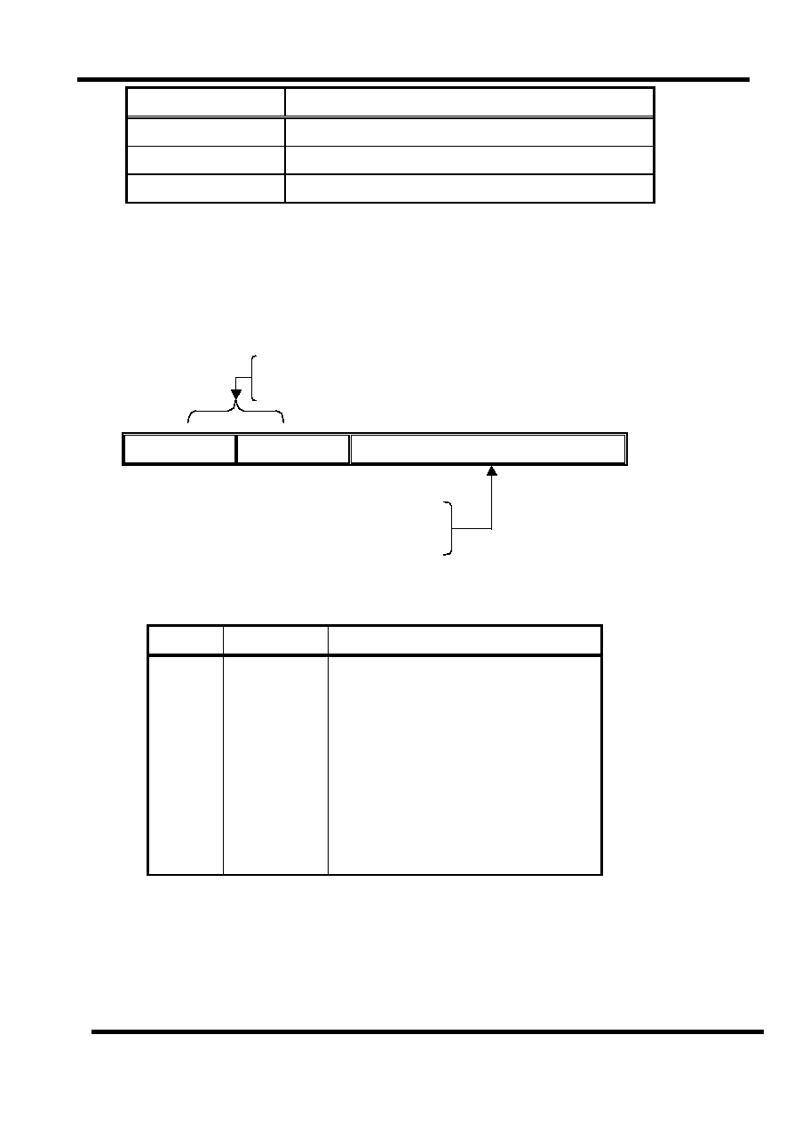
6. Memory Map
(A) Register Map
Address
Description
BANK0
00
Indirect Addressing Register
01
RTCC
02
PCL
03
STATUS
04
MSR
05
Port A
06
Port B
08
ADS0
09
ADRES
0A
PCH
0B
INTS
0C~4F
General purpose register
BANK1
01
TMR
05
CPIO A
MDT2051
This specification are subject to be changed without notice. Any latest information please preview
http;//www.mdtic.com.tw
P. 3
2004/1 Ver. 1.8
Address
Description
06
CPIO B
07
PSTA
08
ADS1
(1)IAR ( Indirect Address Register) : R00
(2)RTCC (Real Time Counter/Counter Register) : R01
(3) PC (Program Counter) : R02,R0A
Write PC --- from PCH
LJUMP, LCALL --- from instruction word
RTIW, RET,RTFI --- from STACK
A9
A8
A7~A0
Write PC --- from ALU
LJUMP, LCALL --- from instruction word
RTIW, RET, RTFI --- from STACK
(4) STATUS (Status register) : R03
Bit
Symbol
Function
0
1
2
3
4
5
7~6
C
HC
Z
PF
TF
RBS0
----
Carry bit
Half Carry bit
Zero bit
Power down Flag bit
WDT Timer overflow Flag bit
Register Bank Select bit :
0 : 00H --- 7FH
1 : 80H --- FFH
General purpose bit
MDT2051
This specification are subject to be changed without notice. Any latest information please preview
http;//www.mdtic.com.tw
P. 4
2004/1 Ver. 1.8
(5) MSR (Memory Bank Select Register) : R4
Memory Bank Select Register :
0 : 00~7F
1 : 80~FF
b7
b6
b5
b4
b3
b2
b1
b0
Indirect Addressing Mode
(6) PORT A : R05
PA4~PA0, I/O Register
(7) PORT B : R06
PB7~PB0, I/O Register
(8) ADS0 ( A/D Status Register ) : R08
Bit
Symbol
Function
0
ADRUN
0 : A/D converter module is shut off and consumes no operating current
1 : A/D converter module is operating
1
ADIF
A/D conversion complete interrupt flag bit
Set when conversion is completed. Reset in software.
2
GO/DONEB
GO/DONEB must be set to begin a conversion . It is automatically reset
in hardware when the conversion is complete
4,3
CHS1-0
00 : AIC0 01 : AIC1 10 : AIC2 11 : AIC3
5
Reserved
Can be used as a general purpose r/w bit
7,6
ASCS1-0
00 : fosc/2 01: fosc/8 10 : fosc/32 11 : f RC (*Note)
*Note: determined by OSC mode, HF: fosc/32 XT: fosc/8 RC: fosc/2 LF: fosc/2
(9) ADRES ( A/D result register ) : R09
(10)PCH (High byte of PC) : R0A
Bit
Function
1~0
High byte of PC
7~2
Unimplemented, reads as
`
0
'

MDT2051
This specification are subject to be changed without notice. Any latest information please preview
http;//www.mdtic.com.tw
P. 5
2004/1 Ver. 1.8
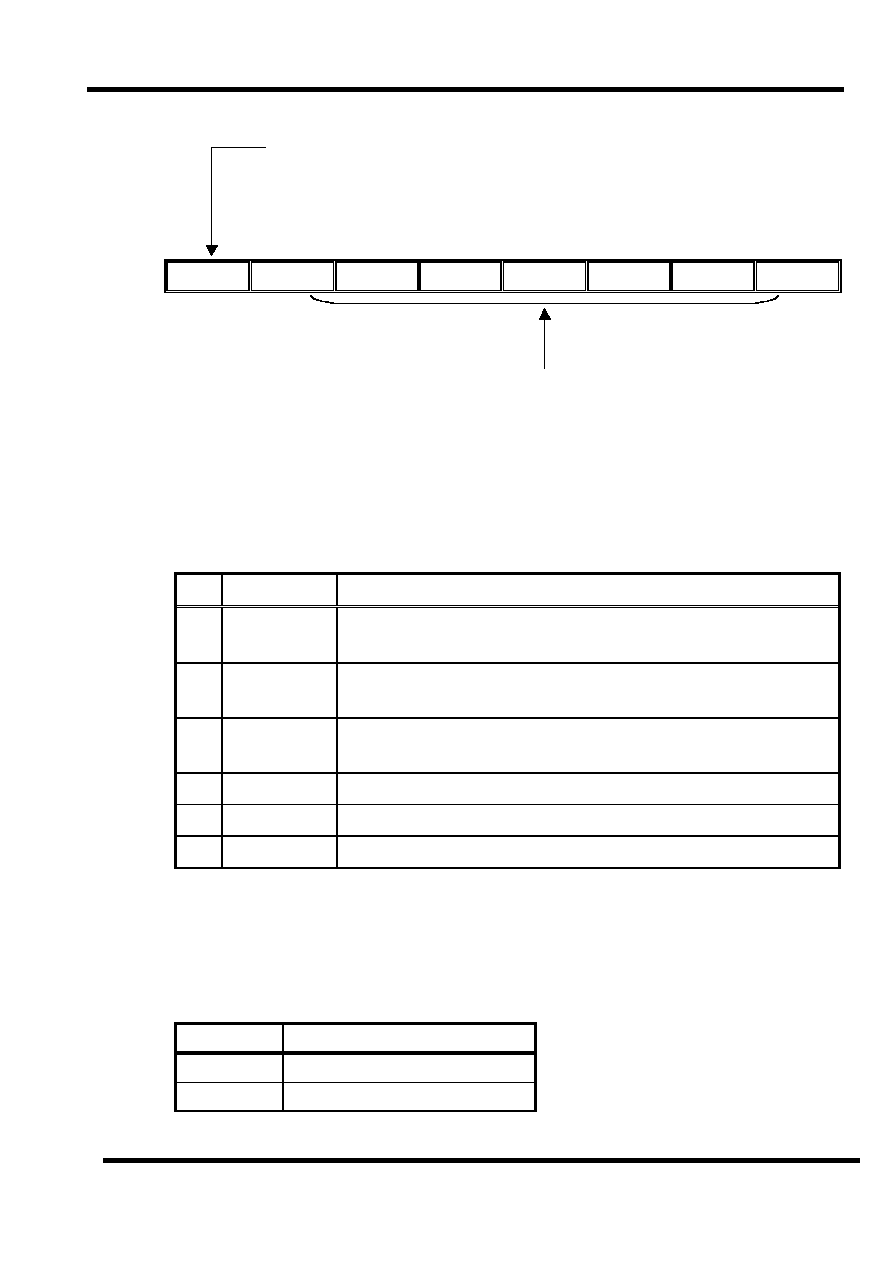
(11) INTS ( Interrupt Status Register ) : R0B
Bit
Symbol
Function
0
RBIF
PORT B change interrupt flag. Set when PB <7:4> inputs change
1
INTF
Set when INT interrupt occurs. INT interrupt flag.
2
TIF
Set when TMR overflows.
3
RBIE
0 : disable PB change interrupt
1 : enable PB change interrupt
4
INTS
0 : disable INT interrupt
1 : enable INT interrupt
5
TIS
0 : disable TMR interrupt
1 : enable TMR interrupt
6
ADIS
0 : disable A/D interrupt
1 : enable A/D interrupt
7
GIS
0 : disable global interrupt
1 : enable global interrupt
(12) TMR (Time Mode Register) : R81
Bit
Symbol
Function
Prescaler Value
RTCC rate
WDT rate
2
--
0
PS2
--
0
0 0 0
0 0 1
0 1 0
0 1 1
1 0 0
1 0 1
1 1 0
1 1 1
1 : 2
1 : 4
1 : 8
1 : 16
1 : 32
1 : 64
1 : 128
1 : 256
1 : 1
1 : 2
1 : 4
1 : 8
1 : 16
1 : 32
1 : 64
1 : 128
3
PSC
Prescaler assignment bit :
0
--
RTCC
1
--
Watchdog Timer
4
TCE
RTCC signal Edge :
0
--
Increment on low-to-high transition on RTCC pin
1
--
Increment on high-to-low transition on RTCC pin
5
TCS
RTCC signal set :
0
--
Internal instruction cycle clock
1
--
Transition on RTCC pin
6
IES
Interrupt edge select
0
--
Interrupt on falling edge on PB0
1
--
Interrupt on rising edge on PB0
7
PBPH
PORTB pull-hi
0
--
PORTB pull-hi are enable
1
--
PORTB pull-hi are disable