PRELIMINARY
Page 1 of 13 Specifications subject to change without notice. US Patent No.6,822,321
Rev. 3
http://www.cree.com/
PFM21030
SPECIFICATION
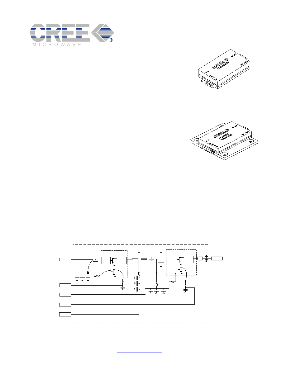
2110-2170 MHz, 30W, 2-Stage Power Module
Enhancement-Mode Lateral MOSFETs
This versatile UMTS module provides excellent linearity and efficiency in
a low-cost surface mount package. The PFM21030 includes two stages
of amplification, along with internal sense FETs that are on the same
silicon die as the RF devices. These thermally coupled sense FETs
simplify the task of bias temperature compensation of the overall amplifier.
The module includes RF input, interstage, and output matching elements.
The source and load impedances required for optimum operation of the
module are much higher (and simpler to realize) than for unmatched Si
LDMOS transistors of similar performance.
The surface mount package base is typically soldered to a conventional
PCB pad with an array of via holes for grounding and thermal sinking
of the module. Optimized internal construction supports low FET
channel temperature for reliable operation.
� 27 dB Gain
� 30 Watts Peak Output Power
� Internal Tracking FETs
(for improved bias control)
� WCDMA Performance
5 Watts Average Output Level
18% Power Added Efficiency
�45 dBc ACPR
Module Schematic Diagram
Note: Additionally, there are 250K Ohm resistors connected in shunt with all leads, to enhance ESD protection.
Gate 1
RF IN
Sense S1
Gate 2
Sense S2
D1
Drain 2
RF OUT
Lead
Lead
Lead
Lead
Lead
Lead
Q1
Input
Match
Q2
Input
Match
Output
Match
S1
Q1 Die Carrier
Q2 Die Carrier
Module Substrate
S2
Output
Match
Package Type: Surface Mount
PN: PFM21030SM
Package Type: Flange
PN: PFM21030F

PFM21030
Page 2 of 13 Specifications subject to change without notice. U.S. Patent No.6,822,321
Rev. 2
http://www.cree.com/
Electrical Specification
Parameter
Limits
Units
Comments
Min
Typ
Max
1
Operating
Frequency
2110 - 2170
MHz
2 Gain
25 26.7 30
dB Note
1.
3
Gain Compression at
Pout =30 Watts
- 1.3 2.0 dB
Pulsed CW compression measurement
(12
�sec pulse, 120 �sec period, 10%
duty cycle).
4
Gain Flatness over any
30 MHz bandwidth
-
� 0.1
� 0.3
dB
5
Deviation from Linear
Phase over any 30
MHz bandwidth
-
� 1.0
� 2.0
�
6 Group
Delay
-
3.5
3.8 nanosec
Includes delay of test fixture (~0.6
nanoseconds).
7
ACPR with WCDMA
Pave = 5 W
-40 -44 - dBc
Note 3. Refer to applications data for
performance with other protocols.
8
Efficiency under
WCDMA Protocol,
Pave = 5 W
17
19
-
%
Note 3.
9
Efficiency @ 30W
CW Output
40 - %
10
DC Drain Supply
Voltage
24 27 30
Volts
Testing for conformance with RF
specifications is at +27 V.
11
Operating
Temperature Range
(base temperature)
-40 - +115
�C
Testing for conformance with RF
specification is at +25
�C.
12
Gain Variation versus
Temperature
- -0.033 - dB/
�C Bias quiescent currents held constant.
13
Output Mismatch
Stress
- - 30
Watts
CW
VSWR 10:1, all phase angles. No
degradation in output power before &
after test.
14 Stability
-60
-
-
dBc
0<Pout<44.8 dBm CW, 3:1 VSWR
15 Theta jc (channel)
-
-
2.1
�C/W
Theta jc is for output device. Verified
with IR scan. Note 2.
16
Quiescent Currents
a) Q1
b) Q2
80
240
mA
mA
These DC quiescent currents are typical
of the levels that produce optimum
linearity for CDMA protocol.
17
Tracking FET
Periphery Ratio
a) Stg
1
Track
b) Stg
2
Track
3.0
1.7
%
%
Ratio of sense FET current, relative to RF
FET current. Ratios are: Stg 1: 33:1;
Stg 2: 58:1 Gates of sense & RF FETs
are DC connected. Measured with no RF
signal present.
18
ESD Protection
a) Human Body Model
b) Machine Model
Class 1
Class M3
a) 2000V, 100 pF, 1500 Ohms
b) 400V, 200 pF, zero Ohms
Mil STD 883E, Method 3015 for Human
Body Model and for Machine Model.

PFM21030
Page 3 of 13 Specifications subject to change without notice. U.S. Patent No.6,822,321
Rev. 2
http://www.cree.com/
Electrical Specification (Continued)
MAXIMUM RATINGS
Rating
Symbol
Value
Units
19
DC Drain Supply
a) Drain-to-Source
Voltage,
(V
GS
=0), D1 & D2
& Track D1 & Track D2
b) Normal Operation (Class AB operation)
V
DS
V
D_SUPPLY
+50
+30
Volts DC
Volts DC
20
DC Gate Supply
a) Gate-to-source
Voltage
(V
DS
=0)
Normal Operation (Class AB operation)
V
GS
V
G_SUPPLY
-0.5<V
GS
<+15
0<V
GS
<+6
Volts DC
Volts DC
21
RF Input Power
P
IN
+25 dBm
22
Maximum Power Dissipation (T
+85 �C)
a) Derate above +85
�C base temperature.
P
TOTAL
65
-0.7
Watts
Watts/
�C
23
Maximum Channel Operating Temperature
T
CH
+200
�C
24
Storage Temperature Range
T
STG
-40 to +150
�C
RECOMMENDED SOURCE AND LOAD IMPEDANCES
Impedance Units
Comments
Nominal Source
Impedance for
Optimum Operation
18.3 � j0.1
Ohms
Matched for optimum linearity and gain flatness. Impedance
is looking from the module input lead into the input matching
circuit. Reference plane is 0.105 inches from input end of
module.
Nominal Load
Impedance for
Optimum Operation
23.7 + j3.8
Ohms
Matched for optimum efficiency under WCDMA protocol.
Impedance is from the module output lead looking into the
output matching circuit. Reference plane is 0.105 inches from
output end of module.
Specification Notes:
1) The module is mounted in a test fixture with external matching elements for all testing. Quiescent current bias
conditions are those appropriate for minimum ACPR under CDMA protocol. Supply voltage for all tests is
+27 volts DC. Testing is at +25
�C unless otherwise specified.
2) Theta jc is measured with a package mounting (base) temp of +85
�C, and with 10 Watts CW output.
3) Pout=5 Watts average; WCDMA protocol:
(3GPP Test Model 1, 64 DPCH.)
.
ACPR conditions: 5.00 MHz offset, 3.84 MHz BW (crest factor = 11 dB).
4) Sense FETs are scaled versions of the main RF FETs, formed from electrically isolated cells at end of the RF
structure. Current scales according to periphery (threshold voltages offset is less than
�150 millivolts between
adjacent devices). RF & Sense FET gates and sources are DC connected. Drains are DC isolated. Leads S1 & S2
are DC connected to drains of sense FETs 1 & 2. Sources are connected to package base. Sense FETs are
electrically isolated from the RF signals.
PFM21030
Page 4 of 13 Specifications subject to change without notice. U.S. Patent No.6,822,321
Rev. 2
http://www.cree.com/
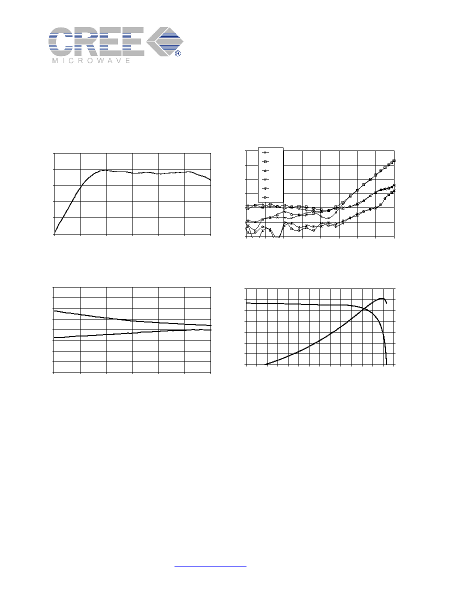
Typical Module Performance
T=+25
�C, unless otherwise noted. Data is for module in a test fixture with external matching elements. See following
page for test fixture details.
Note: The above data is for initial prototype units. Consult the factory for latest data.
Typical CW 2-Tone Intermods vs. Output Power
-70
-60
-50
-40
-30
-20
-10
27
29
31
33
35
37
39
41
43
Average Output Power (dBm)
I
n
t
e
r
m
o
d
R
e
je
c
t
io
n
(
d
B
c
)
IM3L
IM3U
IM5L
IM5U
IM7L
IM7U
Typical Small-Signal Gain vs. Frequency
23
24
25
26
27
28
1990
2050
2110
2170
2230
2290
2350
Frequency (MHz)
G
a
in (
d
B
)
Typical Gain & Efficiency vs CW Output Power
21
22
23
24
25
26
27
28
32
33
34
35
36
37
38
39
40
41
42
43
44
45
46
Output Power (dBm)
G
a
in (
d
B
)
10
15
20
25
30
35
40
45
E
ffi
ci
e
n
cy (%
)
GAIN
EFFICIENCY
Typical Input & Output Return Loss vs Freq.
- 1 6
- 1 4
- 1 2
- 1 0
- 8
- 6
- 4
- 2
0
2 0 5 0
2 0 8 0
2 1 1 0
2 1 4 0
2 1 7 0
2 2 0 0
2 2 3 0
Frequency (MHz)
Ret
u
rn
L
o
ss (
d
B)
OUTPUT
INPUT
PFM21030
Page 5 of 13 Specifications subject to change without notice. U.S. Patent No.6,822,321
Rev. 2
http://www.cree.com/
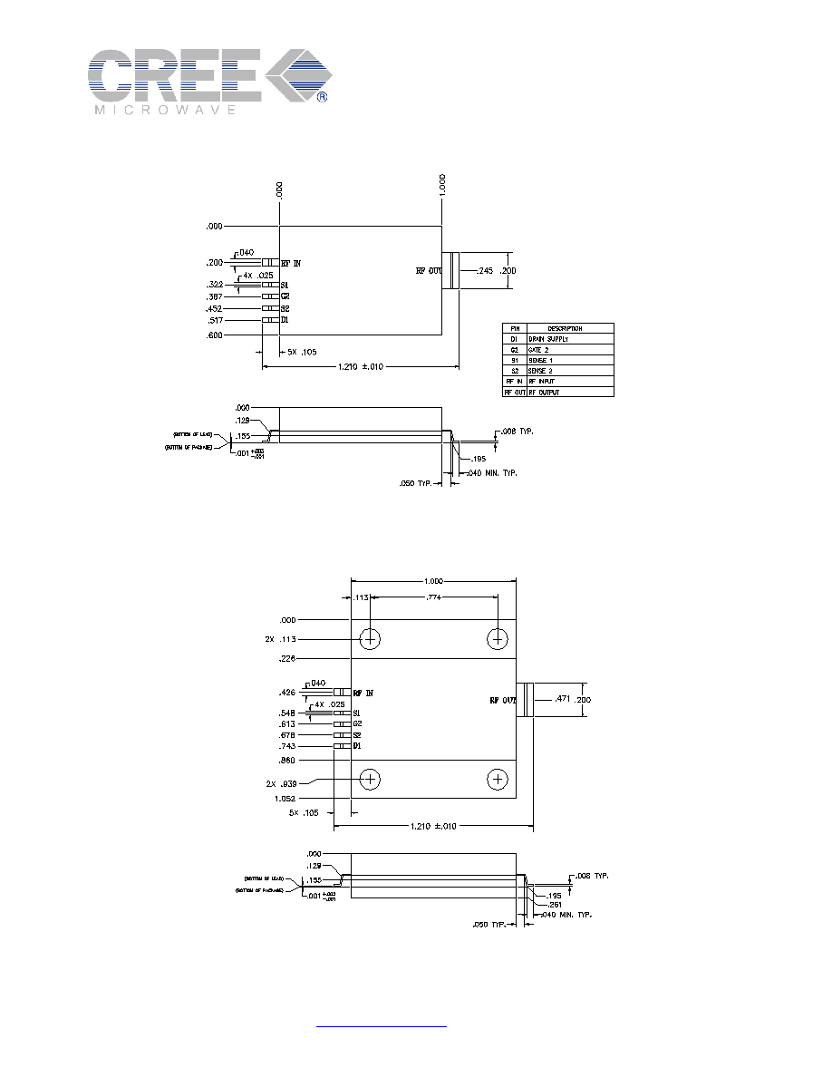
PFM21030SM Package Outline
PFM21030F Package Outline