 | ÐлекÑÑоннÑй компоненÑ: SFP70N06 | СкаÑаÑÑ:  PDF PDF  ZIP ZIP |
Äîêóìåíòàöèÿ è îïèñàíèÿ www.docs.chipfind.ru
Absolute Maximum Ratings
Symbol
Parameter
Value
Units
V
DSS
Drain to Source Voltage
60
V
I
D
Continuous Drain Current(@T
C
= 25
°C)
70
A
Continuous Drain Current(@T
C
= 100
°C)
51
A
I
DM
Drain Current Pulsed
(Note 1)
280
A
V
GS
Gate to Source Voltage
±25
V
E
AS
Single Pulsed Avalanche Energy
(Note 2)
800
mJ
dv/dt
Peak Diode Recovery dv/dt
(Note 3)
7.0
V/ns
P
D
Total Power Dissipation(@T
C
= 25 °C)
158
W
Derating Factor above 25 °C
1.05
W/°C
T
STG,
T
J
Operating Junction Temperature & Storage Temperature
- 55 ~ 175
°C
T
L
Maximum Lead Temperature for soldering purpose,
1/8 from Case for 5 seconds.
300
°C
Thermal Characteristics
Symbol
Parameter
Value
Units
Min.
Typ.
Max.
R
JC
Thermal Resistance, Junction-to-Case
-
-
0.95
°C/W
R
CS
Thermal Resistance, Case to Sink
-
0.5
-
°C/W
R
JA
Thermal Resistance, Junction-to-Ambient
-
-
62.5
°C/W
SFP70N06
1/7
Features
Low R
DS
(on) (0.015 )@V
GS
=10V
Low Gate Charge (Typical 65nC)
Low Crss (Typical 150pF)
Improved dv/dt Capability
100% Avalanche Tested
Maximum Junction Temperature Range (175°C)
General Description
This Power MOSFET is produced using Wisdom's advanced
planar stripe, DMOS technology. This latest technology has been
especially designed to minimize on-state resistance, have a low
gate charge with superior switching performance, and rugged
avalanche characteristics. This Power MOSFET is well suited
for synchronous DC-DC Converters and Power Management in
portable and battery operated products.
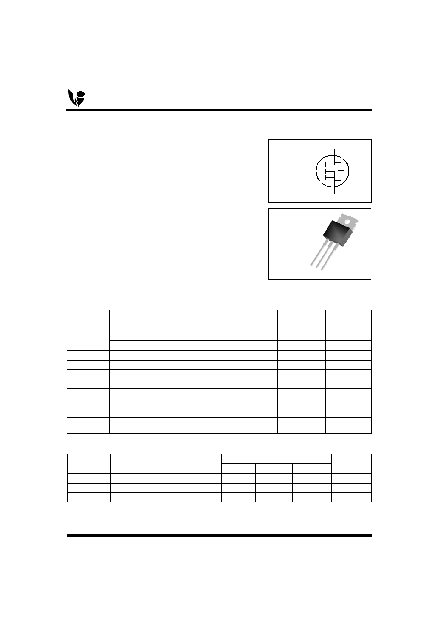
N-Channel MOSFET
TO-220
1 2
3
Symbol
2. Drain
3. Source
1. Gate
Wisdom
Technologies Int'l
June, 2004. Rev. 0.
Copyright@Wisdom Technologies International, All rights reserved.
SFP70N06
Electrical Characteristics
( T
C
= 25 °C unless otherwise noted )
Symbol
Parameter
Test Conditions
Min
Typ
Max
Units
Off Characteristics
BV
DSS
Drain-Source Breakdown Voltage
V
GS
= 0V, I
D
= 250uA
60
-
-
V
BV
DSS
/
T
J
Breakdown Voltage Temperature
coefficient
I
D
= 250uA, referenced to 25 °C
-
0.06
-
V/°C
I
DSS
Zero Gate Voltage Drain Current
V
DS
= 60V, V
GS
= 0V
-
-
1
uA
V
DS
= 48V, T
C
= 150 °C
-
-
10
uA
I
GSS
Gate-Source Leakage, Forward
V
GS
= 25V, V
DS
= 0V
100
nA
Gate-Source Leakage, Reverse
V
GS
= -25V, V
DS
= 0V
-
-
-100
nA
On Characteristics
V
GS(th)
Gate Threshold Voltage
V
DS
= V
GS
, I
D
= 250uA
2.0
-
4.0
V
R
DS(ON)
Static Drain-Source On-state Resis-
tance
V
GS
=10 V, I
D
= 35A
-
0.013
0.015
Dynamic Characteristics
C
iss
Input Capacitance
V
GS
=0 V, V
DS
=25V, f = 1MHz
-
2200
2900
pF
C
oss
Output Capacitance
-
650
850
C
rss
Reverse Transfer Capacitance
-
150
195
Dynamic Characteristics
t
d(on)
Turn-on Delay Time
V
DD
=30V, I
D
=35A, R
G
=50
see fig. 13.
(Note 4, 5)
-
30
70
ns
t
r
Rise Time
-
60
130
t
d(off)
Turn-off Delay Time
-
125
260
t
f
Fall Time
-
95
200
Q
g
Total Gate Charge
V
DS
=48V, V
GS
=10V, I
D
=70A
see fig. 12.
(Note 4, 5)
-
65
85
nC
Q
gs
Gate-Source Charge
-
17
-
Q
gd
Gate-Drain Charge(Miller Charge)
-
23
-
Source-Drain Diode Ratings and Characteristics
Symbol
Parameter
Test Conditions
Min.
Typ.
Max.
Unit.
I
S
Continuous Source Current
Integral Reverse p-n Junction
Diode in the MOSFET
-
-
70
A
I
SM
Pulsed Source Current
-
-
280
V
SD
Diode Forward Voltage
I
S
=70A, V
GS
=0V
-
-
1.5
V
t
rr
Reverse Recovery Time
I
S
=70A,V
GS
=0V,dI
F
/dt=100A/us
-
62
-
ns
Q
rr
Reverse Recovery Charge
-
110
-
nC
NOTES
1. Repeativity rating : pulse width limited by junction temperature
2. L = 250 uH, I
AS
= 70A, V
DD
= 25V, R
G
= 0 , Starting T
J
= 25°C
3. ISD 70A, di/dt 300A/us, V
DD
BV
DSS
, Starting T
J
= 25°C
4. Pulse Test : Pulse Width 300us, Duty Cycle 2%
5. Essentially independent of operating temperature.
2/7
Copyright@Wisdom Technologies International, All rights reserved.
0.2
0.4
0.6
0.8
1.0
1.2
1.4
1.6
1.8
10
0
10
1
10
2
175
Notes :
1. V
GS
= 0V
2. 250µ s Pulse Test
25
I
DR
,
R
e
v
e
rse Dra
i
n Cu
rren
t
[A
]
V
SD
, Source-Drain voltage [V]
0
50
100
150
200
250
300
0
5
10
15
20
25
30
V
GS
= 10V
V
GS
= 20V
Note : T
J
= 25
R
DS
(
O
N)
,
Drai
n-S
o
urce
On-R
esi
s
t
a
nce
[m
]
I
D
, Drain Current [A]
2
4
6
8
10
10
0
10
1
10
2
175
o
C
25
o
C
-55
o
C
Notes :
1. V
DS
= 25V
2. 250µ s Pulse Test
I
D
,
Dr
ai
n Cur
r
ent
[
A
]
V
GS
, Gate-Source Voltage [V]
10
-1
10
0
10
1
10
0
10
1
10
2
V
GS
Top : 15.0 V
10.0 V
8.0 V
7.0 V
6.0 V
5.5 V
5.0 V
Bottom : 4.5 V
Notes :
1. 250µ s Pulse Test
2. T
C
= 25
I
D
,
Drai
n
Cur
r
ent
[
A
]
V
DS
, Drain-Source Voltage [V]
0
10
20
30
40
50
60
70
0
2
4
6
8
10
12
V
DS
= 30V
V
DS
= 48V
Note : I
D
= 70.0 A
V
GS
,
Gate-S
o
u
rce
V
o
ltage [
V
]
Q
G
, Total Gate Charge [nC]
0
5
10
15
20
25
30
35
0
500
1000
1500
2000
2500
3000
3500
4000
4500
5000
5500
C
rss
C
oss
C
iss
Notes :
1. V
GS
= 0V
2. f=1MHz
C
iss
=C
gs
+C
gd
(C
ds
=shorted)
C
oss
=C
ds
+C
gd
C
rss
=C
gd
C
a
pa
c
i
ta
nc
e
[p
F]
V
DS
, Drain-Source Voltage [V]
3/7
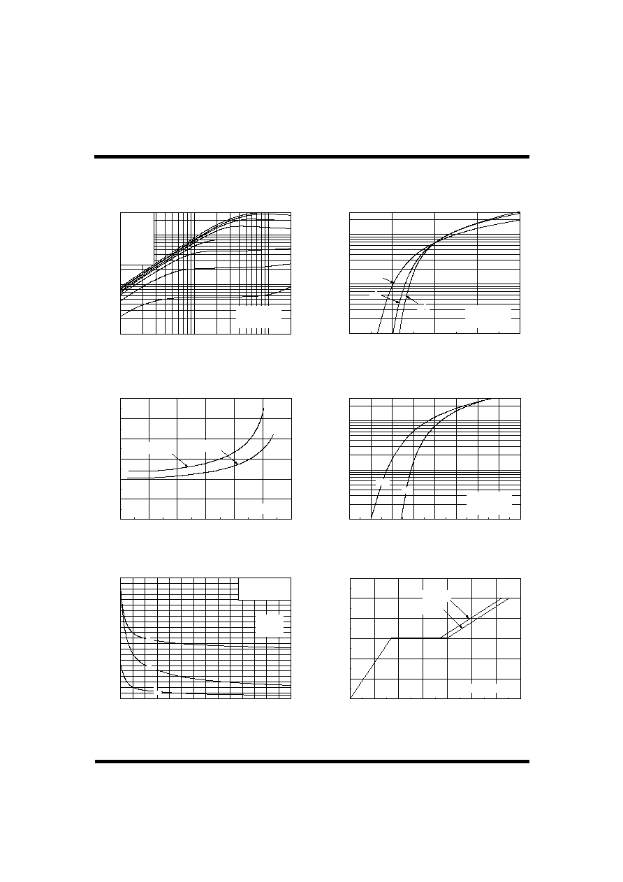
Fig 3. On Resistance Variation vs.
Drain Current and Gate Voltage
Fig 4. On State Current vs.
Allowable Case Temperature
Fig 5. Capacitance Characteristics
Fig 6. Gate Charge Characteristics
SFP70N06
Fig 1. On-State Characteristics
Fig 2. Transfer Characteristics
Copyright@Wisdom Technologies International, All rights reserved.
10
-1
10
0
10
1
10
2
10
0
10
1
10
2
10
3
DC
10 ms
1 ms
100 µs
Operation in This Area
is Limited by R
DS(on)
Notes :
1. T
C
= 25
o
C
2. T
J
= 175
o
C
3. Single Pulse
I
D
, Dr
ai
n C
u
r
r
e
n
t [A]
V
DS
, Drain-Source Voltage [V]
1 0
-5
1 0
-4
1 0
-3
1 0
-2
1 0
-1
1 0
0
1 0
1
1 0
-2
1 0
-1
1 0
0
N o te s :
1 . Z
J C
(t) = 0 .9 5
/W M a x .
2 . D u ty F a c to r, D = t
1
/t
2
3 . T
J M
- T
C
= P
D M
* Z
J C
(t)
s in g le p u ls e
D = 0 .5
0 .0 2
0 .2
0 .0 5
0 .1
0 .0 1
Z
JC
(t
)
,
T
h
e
r
m
a
l Re
spon
se
t
1
, S q u a re W a v e P u ls e D u ra tio n [s e c ]
25
50
75
100
125
150
175
0
10
20
30
40
50
60
70
I
D'
D
r
ai
n C
u
r
r
e
n
t
[A]
T
C'
Case Temperature [
o
C]
-100
-50
0
50
100
150
200
0.0
0.5
1.0
1.5
2.0
2.5
3.0
Notes :
1. V
GS
= 10 V
2. I
D
= 35 A
R
DS
(
O
N
)
,
(
N
o
r
m
a
l
i
zed)
D
r
a
i
n-S
o
ur
ce
O
n
-R
e
s
i
sta
nc
e
T
J
, Junction Temperature [
o
C]
-100
-50
0
50
100
150
200
0.8
0.9
1.0
1.1
1.2
Notes :
1. V
GS
= 0 V
2. I
D
= 250 µ A
BV
DS
S
,
(N
ormal
i
z
e
d)
D
r
a
i
n-S
ource B
r
eak
d
o
w
n
V
o
lt
ag
e
T
J
, Junction Temperature [
o
C]
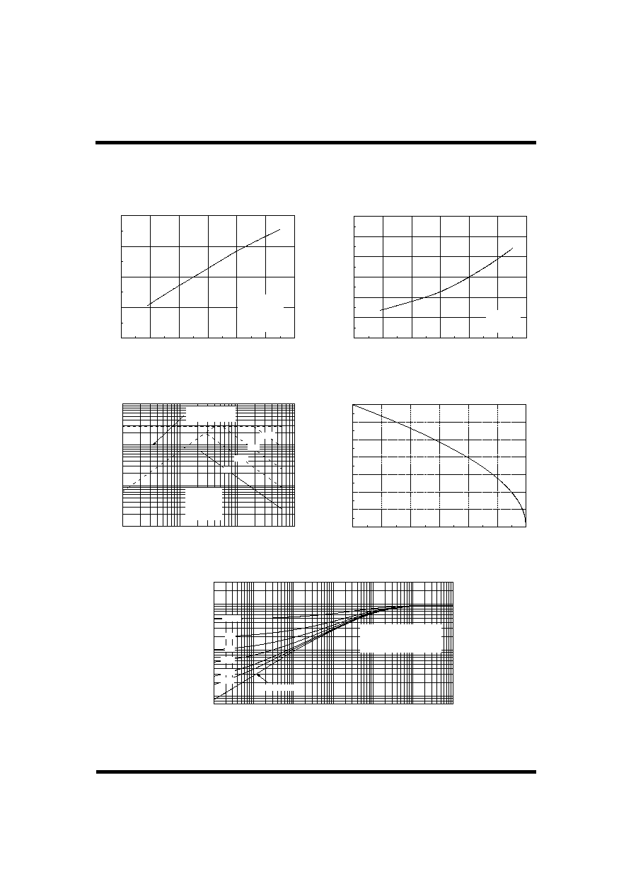
Fig 9. Maximum Safe Operating Area
Fig 10. Maximum Drain Current
vs. Case Temperature
Fig 11. Transient Thermal Response Curve
Fig 7. Breakdown Voltage Variation
vs. Junction Temperature
Fig 8. On-Resistance Variation
vs. Junction Temperature
SFP70N06
4/7
Copyright@Wisdom Technologies International, All rights reserved.
5/7
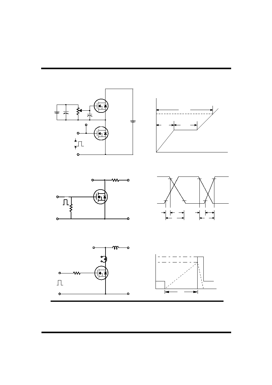
Fig 13. Switching Time Test Circuit & Waveforms
Fig 14. Unclamped Inductive Switching Test Circuit & Waveforms
SFP70N06
Fig. 12. Gate Charge Test Circuit & Waveforms
E
A
S
=
L
L
I
A
S
2
----
2
1
--------------------
B
V
D
S
S
--V
D
D
B
V
D
S
S
E
A
S
=
L
L
I
A
S
2
----
2
1
E
A
S
=
L
L
I
A
S
2
----
2
1
----
2
1
--------------------
B
V
D
S
S
--V
D
D
B
V
D
S
S
V
D
D
V
D
S
B
V
D
S
S
t
p
V
D
D
I
A
S
V
D
S
(t)
I
D
(t)
T
im
e
B
V
D
S
S
t
p
V
D
D
I
A
S
V
D
S
(t)
I
D
(t)
T
im
e
1
0
V
D
U
T
R
G
L
L
I
D
I
D
C
harge
V
G
S
10V
Q
g
Q
gs
Q
gd
1m
A
V
G
S
D
U
T
V
D
S
300nF
50K
200nF
12V
S
am
e Type
as D
U
T
C
harge
V
G
S
10V
Q
g
Q
gs
Q
gd
C
harge
V
G
S
10V
Q
g
Q
gs
Q
gd
1m
A
V
G
S
D
U
T
V
D
S
300nF
50K
200nF
12V
S
am
e Type
as D
U
T
V
in
V
D
S
1
0
%
9
0
%
t
d
(
o
n
)
t
r
t
o
n
t
o
ff
t
d
(
o
ff)
t
f
V
D
D
(
0
.5
r
a
te
d
V
D
S
)
1
0
V
V
D
S
R
L
D
U
T
P
u
ls
e
G
e
n
e
r
a
to
r
V
in
V
D
S
1
0
%
9
0
%
t
d
(
o
n
)
t
r
t
o
n
t
o
ff
t
d
(
o
ff)
t
f
V
in
V
D
S
1
0
%
9
0
%
t
d
(
o
n
)
t
r
t
o
n
t
o
ff
t
d
(
o
ff)
t
f
V
D
D
(
0
.5
r
a
te
d
V
D
S
)
V
V
D
S
R
L
D
U
T
P
u
ls
e
G
e
n
e
r
a
to
r
R
G
V
in
V
D
S
1
0
%
9
0
%
t
d
(
o
n
)
t
r
t
o
n
t
o
ff
t
d
(
o
ff)
t
f
V
in
V
D
S
1
0
%
9
0
%
t
d
(
o
n
)
t
r
t
o
n
t
o
ff
t
d
(
o
ff)
t
f
V
D
D
(
0
.5
r
a
te
d
V
D
S
)
1
0
V
V
D
S
R
L
D
U
T
P
u
ls
e
G
e
n
e
r
a
to
r
V
in
V
D
S
1
0
%
9
0
%
t
d
(
o
n
)
t
r
t
o
n
t
o
ff
t
d
(
o
ff)
t
f
V
in
V
D
S
1
0
%
9
0
%
t
d
(
o
n
)
t
r
t
o
n
t
o
ff
t
d
(
o
ff)
t
f
V
D
D
(
0
.5
r
a
te
d
V
D
S
)
V
V
D
S
R
L
D
U
T
P
u
ls
e
G
e
n
e
r
a
to
r
R
G
Copyright@Wisdom Technologies International, All rights reserved.