Äîêóìåíòàöèÿ è îïèñàíèÿ www.docs.chipfind.ru
The information provided herein is believed to be reliable at press time. Sirenza Microdevices assumes no responsibility for inaccuracies or ommisions. Sirenza Microdevices assumes no responsibility for the use of this information, and all such
information shall be entirely at the user's own risk. Prices and specifications are subject to change without notice. No patent rights or licenses to any of the circuits described herein are implied or granted to any third party. Sirenza Microdevices
does not authorize or warrant any Sirenza Microdevices product for use in life-support devices and/or systems. Copyright 2005 Sirenza Microdevices, Inc. All worldwide rights reserved.
303 S. Technology Court,
Phone: (800) SMI-MMIC
http://www.sirenza.com
Broomfield, CO 80021
1 EDS-104013 Rev D
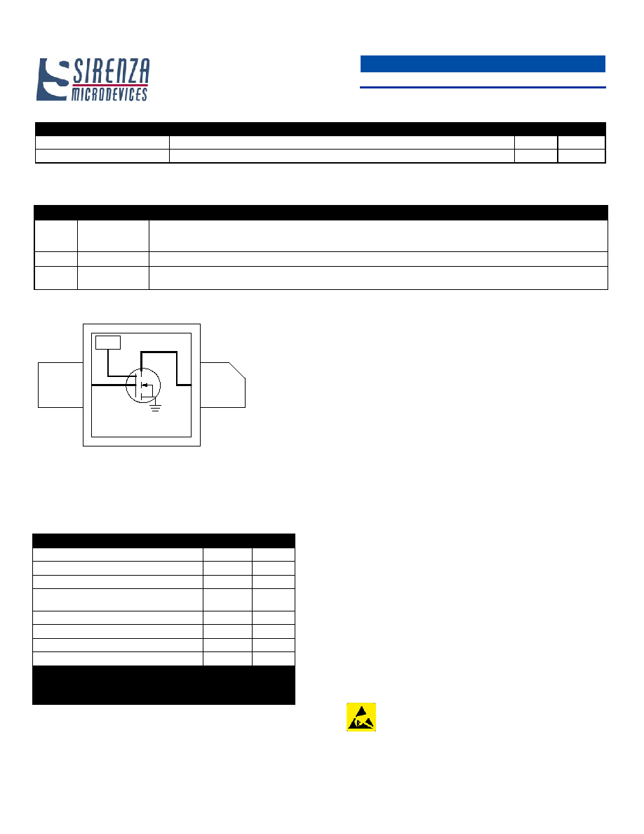
Case Flange = Ground
ESD
Protection
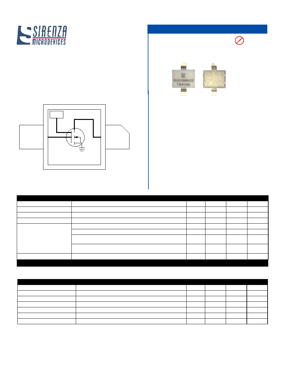
Sirenza Microdevices' SLD-1083CZ is a robust 4 Watt high perfor-
mance LDMOS transistor designed for operation from to 2700MHz. It is
an excellent solution for applications requiring high linearity and effi-
ciency at a low cost. The SLD-1083CZ is typically used in the design of
driver stages for power amplifiers, repeaters, and RFID applica-
tions.The power transistor is fabricated using Sirenza's latest, high per-
formance LDMOS II process.
RF Specifications
Symbol
Parameter
Unit
Min
Typ
Max
Frequency
Frequency of Operation
MHz
-
-
2700
Gain
3 Watt CW, 902-928MHz
dB
18
19
-
Efficiency
Drain Efficiency at 3 Watt CW, 915MHz
%
40
43
-
IRL
Input Return Loss, 3 Watt Output Power, 915MHz
dB
-9.5
-12
-
Linearity
3
rd
Order IMD at 3 Watt PEP (Two Tone), 915MHz
dBc
-
-30
-26
1dB Compression (P
1dB
), 915MHz
Watt
-
4
-
IS-95, 9 Ch Fwd, Offset=750KHz, ACPR Integrated Bandwidth,
ACPR=-55dB
dBm
-
21
-
IS-95, 9 Ch Fwd, Offset=750KHz, ACPR Integrated Bandwidth,
ACPR=-45dB
dBm
-
29
-
R
TH
Thermal Resistance (Junction-to-Case)
ºC/W
11
SLD-1083CZ
4 Watt Discrete LDMOS FET in
Ceramic Package
Product Features
Applications
·
4 Watt Output P
1dB
·
Single Polarity Supply Voltage
·
High Gain: 18 dB at 915 MHz
·
High Efficiency: 47% at 10W CW
·
XeMOS II LDMOS
·
Integrated ESD Protection, Class 1B
·
Base Station PA driver
·
Repeaters
·
RFID
·
Military Communication
·
GSM/CDMA
Product Description
Pb
RoHS Compliant
&
Package
Green
Test Conditions V
DS
= 28.0V, I
DQ
= 30mA, T
Flange
= 25ºC
Functional Schematic Diagram
DC Specifications
Symbol
Parameter
Unit
Min
Typical
Max
g
m
Forward Transconductance @ 30mA I
DS
mA / V
150
V
GS
Threshold
I
DS
=3mA, V
DS
=28V
Volts
4.2
V
DS
Breakdown
1mA V
DS
current
Volts
65
C
iss
Input Capacitance (Gate to Source) V
GS
=0V V
DS
=28V
pF
5.2
C
rss
Reverse Capacitance (Gate to Drain) V
GS
=0V V
DS
=28V
pF
0.2
C
oss
Output Capacitance (Drain to Source) V
GS
=0V V
DS
=28V
pF
3.2
R
DSon
Drain to Source Resistance, V
GS
=10V V
DS
=250mV
3.0
SLD-1083CZ 2700MHz 4 Watt LDMOS FET
303 S. Technology Court
Phone: (800) SMI-MMIC
http://www.sirenza.com
Broomfield, CO 80021
2
EDS-104013 Rev D
Pin Description
Pin #
Function
Description
1
Gate
Transistor RF input and gate bias voltage. The gate bias voltage must be temperature compensated to maintain constant
bias current over the operating temperature range. Care must be taken to protect against video transients that exceed the
maximum input power or voltage.
2
Drain
Transistor RF output and drain bias voltage. Typical voltage 28V.
Flange
Source, Gnd
Exposed area on the bottom side of the package needs to be mechanically attached to the ground plane of the board for
optimum thermal and RF performance. See mounting instructions for recommendation.
Absolute Maximum Ratings
Parameters
Value
Unit
Drain Voltage (V
DS
)
35
Volts
Gate Voltage (V
GS
)
20
Volts
RF Input Power
+30
dBm
Load Impedance for Continuous Operation
Without Damage
10:1
VSWR
Output Device Channel Temperature
+200
ºC
Lead Temperature During Solder Reflow
+270
ºC
Operating Temperature Range
-20 to +90
ºC
Storage Temperature Range
-40 to +100
ºC
Operation of this device beyond any one of these limits may
cause permanent damage. For reliable continuous operation
see typical setup values specified in the table on page one.
Caution: ESD Sensitive
Appropriate precaution in handling, packaging
and testing devices must be observed.
Case Flange = Ground
ESD
Protection
Pin Diagram
Pin 1
Pin 2
Quality Specifications
Parameter
Description
Unit
Typical
ESD Rating
Human Body Model
Volts
750
MTTF
85
o
C Leadframe, 200
o
C Channel
Hours
1.2 X 10
6
Note 1:
Gate voltage must be applied to V
GS
lead concurrently or after
application of drain voltage to prevent potentially destructive
oscillations. Bias voltages should never be applied to the tran-
sistor unless it is properly terminated on both input and output.
Note 2:
The required V
GS
corresponding to a specific I
DQ
will vary from
device to device due to the normal die-to-die variation in thresh-
old voltage withLDMOS transistors.
Note 3:
The threshold voltage (V
GSTH
) of LDMOS transistors varies with
device temperature. External temperature compensation may
be required. See Sirenza application notes AN-067 LDMOS
Bias Temperature Compensation.
SLD-1083CZ 2700MHz 4 Watt LDMOS FET
303 S. Technology Court
Phone: (800) SMI-MMIC
http://www.sirenza.com
Broomfield, CO 80021
3
EDS-104013 Rev D
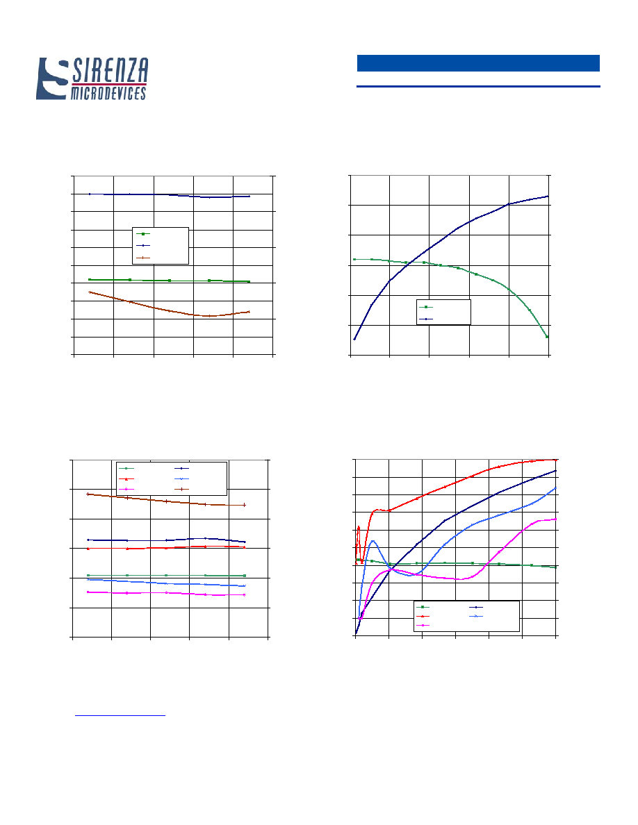
Typical Performance Curves in 900 MHz Application Circuit
CW Gain, Efficiency vs Pout
Vdd=28V, Idq=50mA, Freq=915 MHz
18
19
20
21
22
23
24
0
1
2
3
4
5
Pout (W)
Ga
i
n
(
d
B
)
0
10
20
30
40
50
60
E
ffici
e
n
c
y (
%
)
Gain
Efficiency
2 Tone Gain, Efficiency, Linearity vs Pout
Vdd=28V, Idq=50mA, Freq=915 MHz, Delta F=1 MHz
0
5
10
15
20
25
30
35
40
45
50
0
1
2
3
4
5
6
Pout (W PEP)
G
a
i
n
(
d
B
)
,
E
f
f
i
ci
e
n
cy (
%
)
-70
-65
-60
-55
-50
-45
-40
-35
-30
-25
-20
IM
D
(
d
B
c
)
Gain
Efficiency
IM3
IM5
IM7
2 Tone Gain, Efficiency, Linearity and IRL vs Frequency
Vdd=28V, Idq=50mA, Pout=3W PEP, Delta F=1 MHz
0
10
20
30
40
50
60
900
905
910
915
920
925
Frequency (MHz)
G
a
i
n
(d
B
)
,
E
f
f
i
c
i
e
n
c
y
(%
)
-60
-50
-40
-30
-20
-10
0
IM
D
(
d
B
c
)
,
IR
L
(
d
B
)
Gain
Efficiency
IM3
IM5
IM7
IRL
CW Gain, Efficiency, IRL vs Frequency
Vdd=28V, Idq=50mA, Pout=3W
0
5
10
15
20
25
30
35
40
45
50
900
905
910
915
920
925
Frequency (MHz)
G
a
i
n
(
d
B),
Ef
f
i
c
i
e
n
c
y
(%
)
-20
-16
-12
-8
-4
0
In
p
u
t R
e
tu
rn
L
o
s
s
(
d
B
)
Gain
Efficiency
IRL
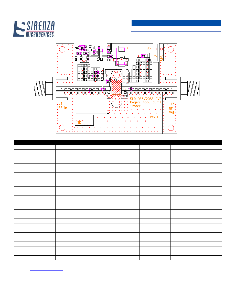
To receive Gerber files, DXF drawings, and assembly recommendations for the test board with fixture, contact applications
support at
support@sirenza.com.
SLD-1083CZ 2700MHz 4 Watt LDMOS FET
303 S. Technology Court
Phone: (800) SMI-MMIC
http://www.sirenza.com
Broomfield, CO 80021
4
EDS-104013 Rev D
Bill of Materials - 900 MHz Application Circuit
Reference Designation
Description
Mfg
Mfg part #
C1
CAP 68PF250V 5% 0603
ATC
600S680JT250XT
C2
CAP 18PF250V 2% 0604
ATC
600S180GT250XT
L1
IND, 16 nH 5% 0603
coilcraft
0603CS-160XJB
L2
IND, 9.5 nH 5% nH 0603
coilcraft
0603CS-9N5XJB
C10
CAP 0.1 UF 16V 10% 0603
AVX
0603YG104ZA2A
C11, C20
CAP 1000 PF 50V 10% 603
AVX
06035C102KAT2A
C12
CAP 68PF 250V 5% 603 LF
ATC
600S680JT250XT
C18
CAP 10 UF 35V 20% TAN T ELECT
Kemet
T494D106M035AS
C19, C22
CAP 0.1 UF 50V 10% 805
Panasonic
ECJ2YB1H104K
J1, J2
Connector SMA END 0.037
Johnson
142-0751-821
J3
Connector MTA SMD R/A 2 PIN
Amp
640455-2
R1
RES 324 1/16W 1% 603
Panasonic
ERJ-3EKF3240V
R2
RES 0 Ohm jumper 805
Panasonic
ERJ6GEY0R00V
R3
POT TRIM 500 OHM 2MM
Panasonic
EVM-2WSX80B52
R30
RES 49.9 1/16W 1% 603
Panasonic
ERJ-EKF49R9V
R5
RES 130 1/16W 1% 603
Panasonic
ERJ-3EKF1300V
R7
RES 210 1/16W 1% 603
Phillips
9C06031A2100FKHFT
R9
RES 0 1/16W 5% 603
Panasonic
ERJ-3GSY0R00V
R90
RES 1.0K 1/16W 1% 603
Panasonic
ERJ-3EKF1001V
RT1
THERMISTOR 100K 5% 603
Panasonic
ERT-J1VV104J
U1
IC VOLT REG 100 MA 5 V SOT-23
National
LM3480IM3-5.0
6 Screws
SCREW #2-56 PHILIPS PAN HEAD
various
-
6 Washers
WASHER #2 FLAT SS
various
-
PCB
PCB, 30 mils thick Dk=3.48
Rogers
4350
Heatsink
machined alumininum
various
-
To receive Gerber files, DXF drawings, and assembly recommendations for the test board with fixture, contact applications
support at
support@sirenza.com.
900 MHz Application Circuit
SLD-1083CZ 2700MHz 4 Watt LDMOS FET
303 S. Technology Court
Phone: (800) SMI-MMIC
http://www.sirenza.com
Broomfield, CO 80021
5
EDS-104013 Rev D
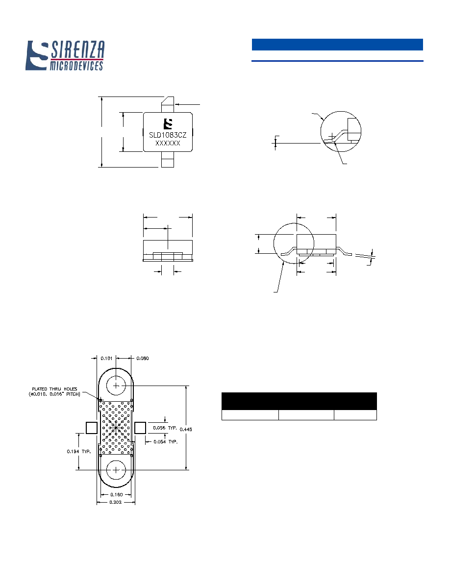
Package Outline Drawing
Recommended Landing Pads for the RF083 Package
All Dimensions are in inches
Part Number Ordering Information
Part Number
Devices Per
Reel
Reel Size
SLD-1083CZ
500
7''
TOP VIEW
SIDE VIEW
END VIEW
0.290
0.160
0.160
0.090
0.160
0.140
0.008
DETAIL A
0.200
0.100
0.050
DETAIL A
0.000±0.002
R0.015
Lead Coplanarity
Lead foot to backside
0.000 ± 0.002
Chamferred Lead
is FET Drain
Document Outline