 | –≠–ª–µ–∫—Ç—Ä–æ–Ω–Ω—ã–π –∫–æ–º–ø–æ–Ω–µ–Ω—Ç: FLK107XV | –°–∫–∞—á–∞—Ç—å:  PDF PDF  ZIP ZIP |
1
Edition 1.3
July 1999
FLK107XV
GaAs FET & HEMT Chips
Item
Saturated Drain Current
Transconductance
Pinch-off Voltage
Gate Source Breakdown Voltage
Power-added Efficiency
Output Power at 1dB
Gain Compression Point
Power Gain at 1dB
Gain Compression Point
Symbol
IDSS
-
400
600
-
200
-
-1.0
-2.0
-3.5
-5
-
-
5.5
6.5
-
-
31
-
29
30
-
VDS = 5V, IDS = 20mA
VDS = 5V, IDS = 250mA
VDS = 5V, VGS = 0V
IGS = -20µA
VDS = 10V
IDS 0.6IDSS
f = 14.5GHz
mA
mS
V
dB
%
dBm
V
gm
Vp
VGSO
P1dB
G1dB
add
Test Conditions
Unit
Limit
Typ.
Max.
Min.
ELECTRICAL CHARACTERISTICS (Ambient Temperature Ta=25∞C)
Note: RF parameter sample size 10pcs. criteria (accept/reject)=(2/3)
Channel to Case
-
15
20
∞C/W
Thermal Resistance
Rth
The chip must be enclosed in a hermetically sealed environment for optimum performance and reliability.
DESCRIPTION
The FLK107XV chip is a power GaAs FET that is
designed for general purpose applications in the Ku-Band
frequency range as it provides superior power, gain, and
efficiency.
Fujitsu's stringent Quality Assurance Program assures the
highest reliability and consistent performance.
Drain
Drain
Drain
Drain
Gate
Gate
Gate
Gate
Item
Drain-Source Voltage
Gate-Source Voltage
Total Power Dissipation
Storage Temperature
Channel Temperature
Symbol
VDS
VGS
15
-5
7.50
-65 to +175
175
Tc = 25∞C
V
V
W
∞C
∞C
Ptot
Tstg
Tch
Condition
Unit
Rating
ABSOLUTE MAXIMUM RATING (Ambient Temperature Ta=25∞C)
Fujitsu recommends the following conditions for the reliable operation of GaAs FETs:
1. The drain-source operating voltage (VDS) should not exceed 10 volts.
2. The forward and reverse gate currents should not exceed 8.8 and -0.5 mA respectively with
gate resistance of 500.
3. The operating channel temperature (Tch) should not exceed 145∞C.
FEATURES
∑ High Output Power: P1dB = 30.0dBm(Typ.)
∑ High Gain: G1dB = 6.5dB(Typ.)
∑ High PAE: add = 31%(Typ.)
∑ Proven Reliability
2
FLK107XV
GaAs FET & HEMT Chips
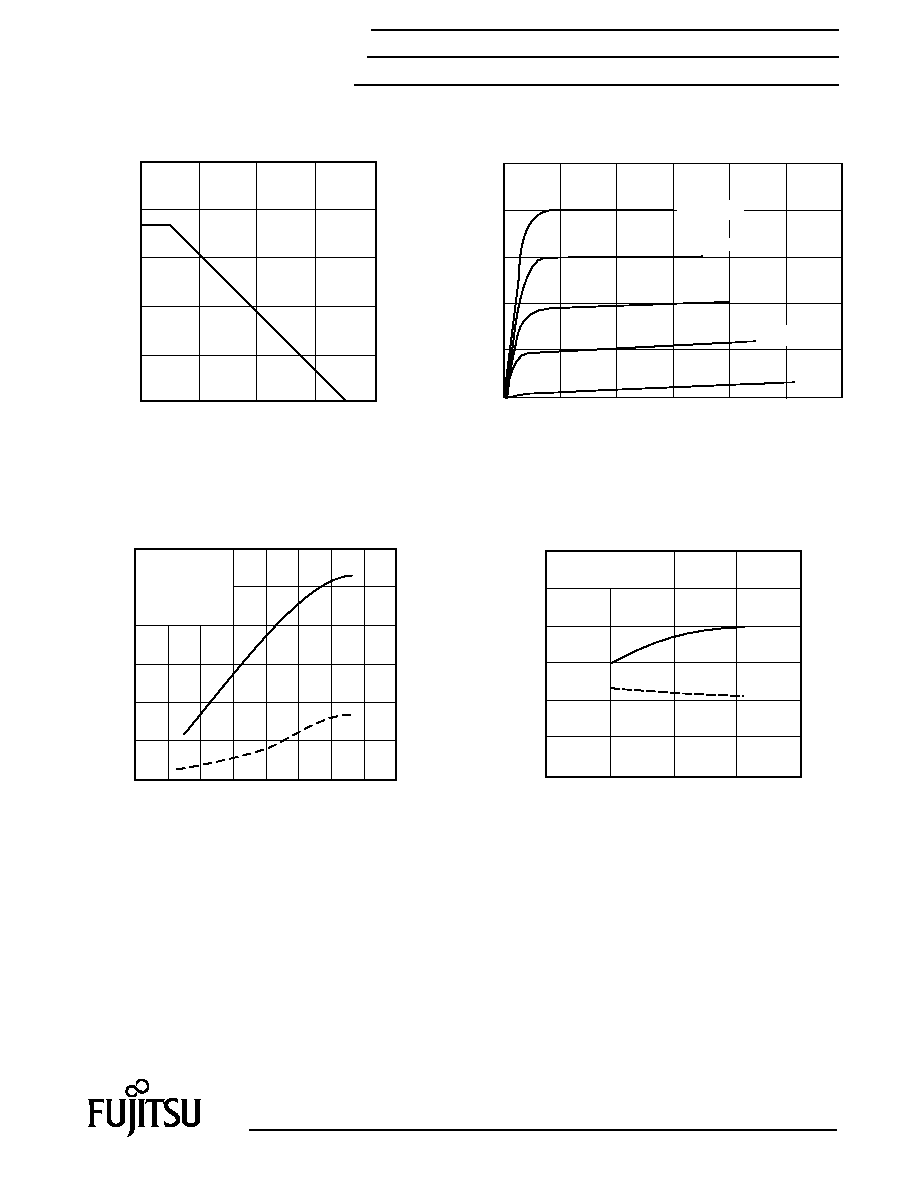
POWER DERATING CURVE
DRAIN CURRENT vs. DRAIN-SOURCE VOLTAGE
4
2
8
10
6
0
50
100
150
200
2
4
6
8
10
Case Temperature (∞C)
Drain-Source Voltage (V)
Total Power Dissipation (W)
30
28
26
24
22
14
16
18
20
22
24
26
Input Power (dBm)
Output Power (dBm)
400
300
200
100
Drain Current (mA)
VGS =0V
-0.5V
-1.5V
-2.0V
-1.0V
OUTPUT POWER vs. INPUT POWER
VDS=10V
IDS0.6IDSS
f = 14.5GHz
add
Pout
40
20
add
(%)
30
31
29
28
27
8
9
10
Drain-Source Voltage (V)
P
1dB
(dBm)
P1dB & add vs. VDS
f = 14.5GHz
IDS0.6IDSS
add
P1dB
30
40
20
add
(%)

3
FLK107XV
GaAs FET & HEMT Chips
S-PARAMETERS
VDS = 10V, IDS = 240mA
FREQUENCY
S11
S21
S12
S22
(MHZ)
MAG
ANG
MAG
ANG
MAG
ANG
MAG
ANG
100
.998
-14.5
11.209
171.6
.007
82.1
.214
-15.0
500
.972
-65.3
9.441
142.2
.031
54.8
.227
-64.9
1000
.941
-105.2
6.826
118.3
.045
33.6
.246
-98.3
1500
.926
-127.5
5.082
103.5
.050
21.4
.263
-113.5
2000
.919
-141.3
3.976
93.0
.052
13.5
.282
-121.0
2500
.915
-150.7
3.236
84.7
.053
7.8
.302
-125.1
3000
.913
-157.5
2.713
77.6
.053
3.3
.324
-127.7
3500
.913
-162.9
2.325
71.3
.053
-0.4
.346
-129.6
4000
.912
-167.3
2.026
65.6
.053
-3.6
.370
-131.1
4500
.913
-171.0
1.789
60.2
.053
-6.4
.394
-132.6
5000
.913
-174.2
1.596
55.1
.052
-8.9
.418
-134.0
5500
.914
-177.1
1.436
50.2
.052
-11.3
.441
-135.4
6000
.915
-179.7
1.301
45.5
.051
-13.5
.465
-136.8
6500
.916
177.9
1.186
41.0
.051
-15.5
.487
-138.3
7000
.917
175.6
1.086
36.6
.050
-17.4
.509
-139.8
7500
.918
173.5
1.000
32.3
.050
-19.2
.530
-141.2
8000
.919
171.5
.923
28.2
.049
-20.9
.551
-142.7
8500
.920
169.6
.856
24.2
.048
-22.5
.570
-144.2
9000
.921
167.7
.795
20.3
.048
-24.0
.589
-145.7
9500
.923
165.9
.741
16.5
.047
-25.5
.607
-147.2
10000
.924
164.2
.692
12.7
.046
-26.8
.624
-148.7
10500
.925
162.5
.648
9.1
.046
-28.2
.640
-150.1
11000
.926
160.9
.608
5.6
.045
-29.4
.655
-151.6
11500
.927
159.3
.572
2.1
.044
-30.6
.669
-153.0
12000
.928
157.7
.538
-1.2
.044
-31.8
.683
-154.4
12500
.929
156.2
.508
-4.5
.043
-32.9
.696
-155.8
13000
.930
154.7
.479
-7.8
.042
-33.9
.708
-157.1
13500
.932
153.2
.453
-10.9
.042
-34.9
.720
-158.5
14000
.933
151.7
.429
-14.0
.041
-35.9
.731
-159.8
14500
.934
150.3
.407
-17.0
.040
-36.8
.741
-161.1
15000
.935
148.9
.386
-19.9
.040
-37.7
.751
-162.3
15500
.936
147.5
.367
-22.8
.039
-38.6
.760
-163.6
16000
.937
146.1
.349
-25.6
.039
-39.4
.769
-164.8
16500
.937
144.8
.333
-28.4
.038
-40.2
.777
-166.0
17000
.938
143.5
.317
-31.1
.038
-41.0
.785
-167.1
17500
.939
142.1
.302
-33.7
.037
-41.7
.793
-168.3
18000
.940
140.8
.289
-36.3
.037
-42.5
.800
-169.4
18500
.941
139.6
.276
-38.8
.036
-43.2
.806
-170.5
19000
.942
138.3
.264
-41.3
.036
-43.8
.813
-171.6
19500
.943
137.1
.252
-43.8
.035
-44.5
.819
-172.7
20000
.944
135.8
.241
-46.2
.035
-45.1
.824
-173.8
NOTE:*
The data includes bonding wires.
n: number of wires
Gate
n=4 (0.2mm length, 25µm Dia Au wire)
Drain n=4 (0.2mm length, 25µm Dia Au wire)
Download S-Parameters, click here
For further information please contact:
FUJITSU COMPOUND SEMICONDUCTOR, INC.
2355 Zanker Rd.
San Jose, CA 95131-1138, U.S.A.
Phone: (408) 232-9500
FAX: (408) 428-9111
www.fcsi.fujitsu.com
FUJITSU MICROELECTRONICS, LTD.
Compound Semiconductor Division
Network House
Norreys Drive
Maidenhead, Berkshire SL6 4FJ
Phone:+44 (0)1628 504800
FAX:+44 (0)1628 504888
Fujitsu Limited reserves the right to change products and specifications without notice.
The information does not convey any license under rights of Fujitsu Limited or others.
© 1998 FUJITSU COMPOUND SEMICONDUCTOR, INC.
Printed in U.S.A. FCSI0598M200
Fujitsu Compound Semiconductor Products contain gallium arsenide
(GaAs) which can be hazardous to the human body and the environment.
For safety, observe the following procedures:
CAUTION
∑ Do not put these products into the mouth.
∑ Do not alter the form of this product into a gas, powder, or liquid
through burning, crushing, or chemical processing as these by-products
are dangerous to the human body if inhaled, ingested, or swallowed.
∑ Observe government laws and company regulations when discarding this
product. This product must be discarded in accordance with methods
specified by applicable hazardous waste procedures.
4
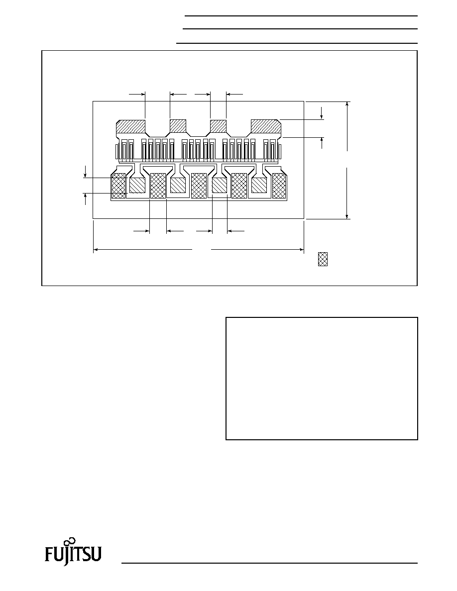
CHIP OUTLINE
Source electrodes are
connected to the PHS
by Via-Hole
Die Thickness: 60±20µm
(Via-Hole)
860
56
55
110
60
480
70
58
Drain
Drain
Drain
Drain
Gate
Gate
Gate
Gate
(Unit: µm)
FLK107XV
GaAs FET & HEMT Chips