Exar Corporation 48720 Kato Road, Fremont CA, 94538 · (510) 668-7000 · FAX (510) 668-7017 · www.exar.com · uarttechsupport@exar.com
áç
áç
áç
áç
XR17C152
5V PCI BUS DUAL UART
APRIL 2002
REV. 1.0.0
GENERAL DESCRIPTION
The XR17C152
1
(152) is a monolithic dual PCI Bus
Universal Asynchronous Receiver and Transmitter
(UART) in Exar's PCI Bus UART family. The device is
designed to meet today's 32-bit PCI Bus and high
bandwidth requirement in communication systems.
The global interrupt source register provides a com-
plete interrupt status indication for both channels to
speed up interrupt parsing. Each UART is indepen-
dently controlled and has its own 16C550 compatible
5G (Fifth Generation) register set, transmit and re-
ceive FIFOs of 64 bytes, fully programmable transmit
and receive FIFO trigger levels, transmit and receive
FIFO level counters, automatic hardware flow control
with programmable hysteresis, automatic software
(Xon/Xoff) flow control, automatic half-duplex control
output, wireless IrDA (Infrared Data Association) in-
frared encoder/decoder, 8 multi-purpose definable in-
puts/outputs, and a 16-bit general purpose timer/
counter.
N
OTE
: 1
Covered by U.S. Patents #5,649,122, #5,832,205
APPLICATIONS
· Network Management
· Factory Automation and Process Control
· Ethernet Network to Serial Ports
· Point-of-Sale Systems
· Remote Access Servers
· Multi serial ports RS-232/RS-422/RS-485 Cards
FEATURES
· High Performance Dual PCI UART
· PCI Bus 2.2 Target Interface Compliance
· 5V PCI Bus Compliant up to 33MHz Clock
· 32-bit PCI Bus Interface with EEPROM Interface
· A Global Interrupt Source Register for both UARTs
· Data Transfer in Byte, Word and Double-word
· Data Read/Write Burst Operation
· Each UART is independently controlled with:
· 16C550 Compatible 5G Register Set
· 64-byte Transmit and Receive FIFOs
· Transmit and Receive FIFO Level Counters
· Automatic RTS/CTS or DTR/DSR Flow Control
· Automatic Xon/Xoff Software Flow Control
· Automatic RS485 Half-duplex Control Output
with 16 Selectable Turn-around Delay
· Infrared (IrDA 1.0) Data Encoder/Decoder
· Programmable Data Rate with Prescaler
· Up to 6.25 Mbps Serial Data Rate at 5V and 8X
Sampling
· Eight Multi-Purpose Inputs/outputs
· A General Purpose 16-bit Timer/Counter
· Sleep Mode with Automatic Wake-up Indicator
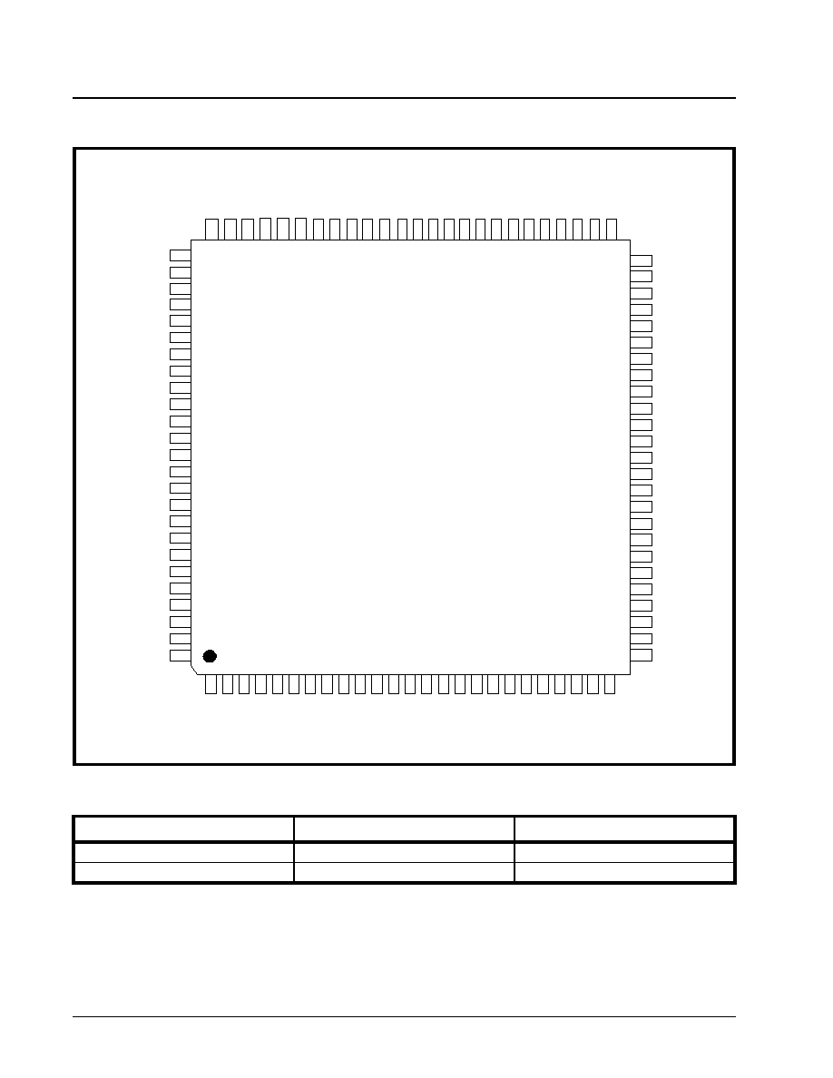
· Low profile 14x14x1.0mm TQFP package
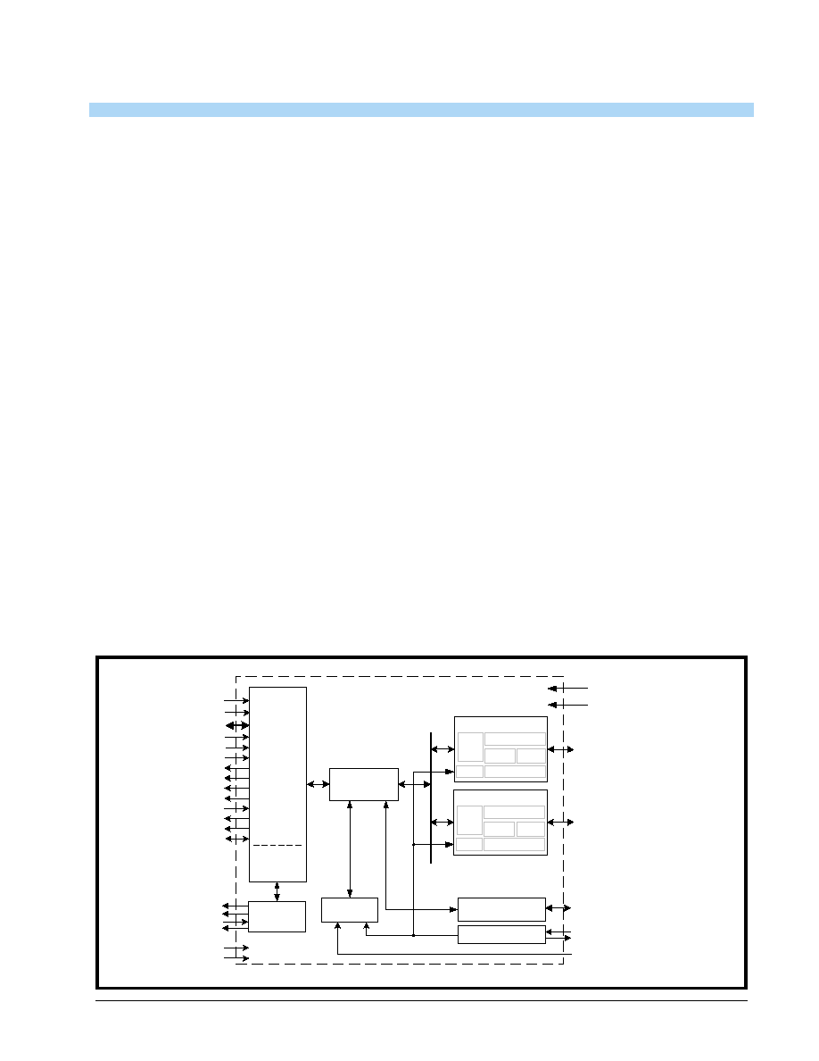
F
IGURE
1. B
LOCK
D
IAGRAM
TMRCK
Device
Configuration
Registers
XTAL1
XTAL2
Crystal Osc/Buffer
TX0, RX0, DTR0#,
DSR0#, RTS0#,
CTS0#, CD0#, RI0#
PCI Local
Bus
Interface
CLK
RST#
AD[31:0]
C/BE[3:0]#
PAR
FRAME#
IRDY#
TRDY#
DEVSEL#
STOP#
IDSEL
PERR#
SERR#
INTA#
Configuration
Space
Registers
.
MPIO0- MPIO7
Multi-purpose
Inputs/Outputs
TX1, RX1, DTR1#,
DSR1#, RTS1#,
CTS1#, CD1#, RI1#
16-bit
Timer/Counter
EECK
EEDI
EEDO
EECS
EEPROM
Interface
5V VCC
GND
ENIR
UART Channel 0
64 Byte TX FIFO
64 Byte RX FIFO
BRG
IR
ENDEC
TX & RX
UART
Regs
UART Channel 1
64 Byte TX FIFO
64 Byte RX FIFO
BRG
IR
ENDEC
TX & RX
UART
Regs
EN485#

áç
áç
áç
áç
XR17C152
5V PCI BUS DUAL UART
REV. 1.0.0
3
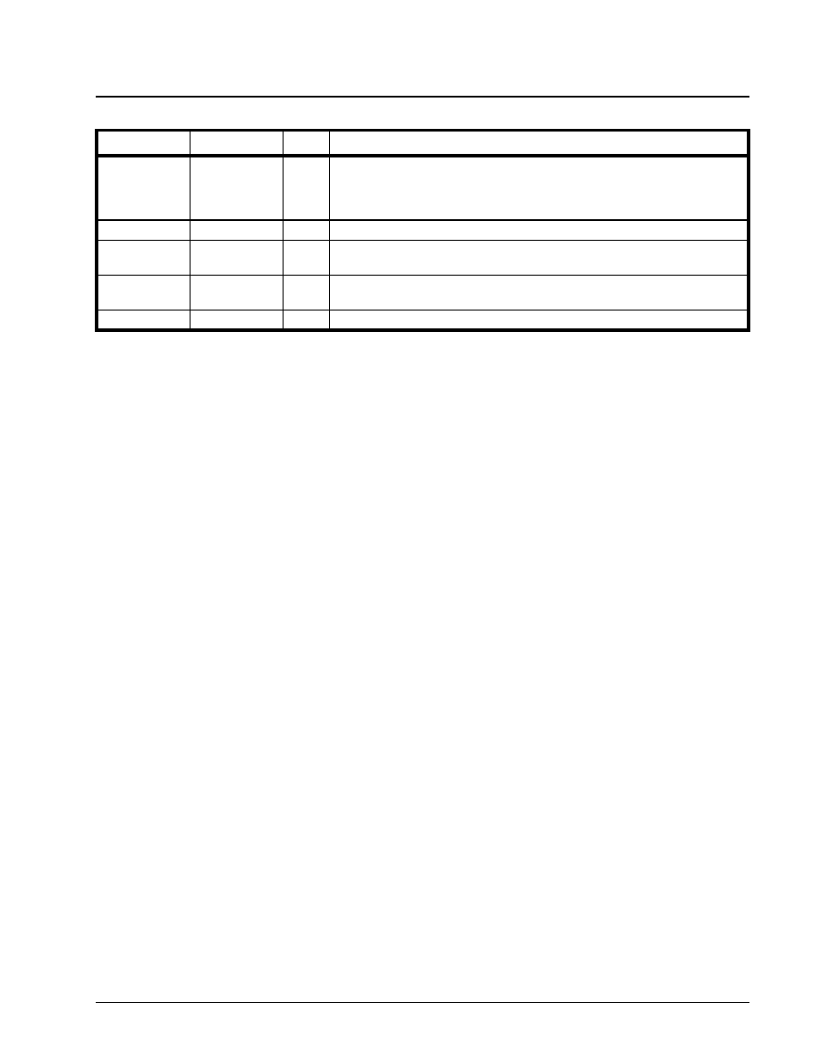
PIN DESCRIPTIONS
Pin Description
N
AME
P
IN
#
T
YPE
D
ESCRIPTION
PCI LOCAL BUS INTERFACE
RST#
86
I
Bus reset input (active low). It resets the PCI local bus configuration space
registers, device configuration registers and UART channel registers to the
default condition, see Table 18.
CLK
87
I
Bus clock input of up to 33MHz at 5V and 22MHz at 3.3V.
AD31-AD0
90-97, 2-9,
24-31, 35-42
I/O
Address data lines [31:0] (bidirectional).
FRAME#
13
I
Bus transaction cycle frame (active low). It indicates the beginning and dura-
tion of an access.
C/BE3#
-
C/BE0#
98, 12,
21, 34
I
Bus Command/Byte Enable [3:0] (active low). This line is multiplexed for bus
Command during the address phase and Byte Enables during the data
phase.
IRDY#
14
I
Initiator Ready (active low). During a write, it indicates that valid data is
present on data bus. During a read, it indicates the master is ready to accept
data.
TRDY#
15
O
Target Ready (active low).
STOP#
17
O
Target request to stop current transaction (active low).
IDSEL
99
I
Initialization device select (active high).
DEVSEL#
16
O
Device select to the XR17C152 (active low).
INTA#
85
OD
Device interrupt from XR17C152 (open drain, active low).
PAR
20
I/O
Parity is even across AD[31:0] and C/BE[3:0]#. (bidirectional, active high).
PERR#
18
O
Data Parity error indicator, except for Special Cycle transactions (active low).
Optional in bus target application.
SERR#
19
OD
System error indicator, Address parity or Data parity during Special Cycle
transactions (open drain, active low). Optional in bus target application.
MODEM OR SERIAL I/O INTERFACE
TX0
73
O
UART channel 0 Transmit Data or infrared transmit data. Normal TXD output
idles at logic 1 condition while infrared TXD output idles at a logic 0 condition.
RX0
66
I
UART channel 0 Receive Data or infrared receive data. Normal RXD input
idles at logic 1 condition while infrared RXD input idles at a logic 0 condition.
In the infrared mode, the polarity of the incoming RXD signal can be selected
via FCTR bit-4. If this bit is a logic 0, logic 0 on the RXD input is considered a
mark and if this bit is a logic 1, a logic 0 on the RXD input is considered a
space.
RTS0#
71
O
UART channel 0 Request to Send or general purpose output (active low). If
this output is not used, leave it unconnected.
CTS0#
67
I
UART channel 0 Clear to Send or general purpose input (active low). This
input should be connected to VCC when not used.
DTR0#
72
O
UART channel 0 Data Terminal Ready or general purpose output (active low).
If this output is not used, leave it unconnected.
DSR0#
68
I
UART channel 0 Data Set Ready or general purpose input (active low). This
input should be connected to VCC when not used.
CD0#
69
I
UART channel 0
Carrier Detect or general purpose input (active low).
This input should be connected to VCC when not used.

XR17C152
áç
áç
áç
áç
5V PCI BUS DUAL UART
REV. 1.0.0
4
RI0#
70
I
UART channel 0 Ring Indicator or general purpose input (active low). This
input should be connected to VCC when not used.
TX1
62
O
UART channel 1 Transmit Data or infrared transmit data. Normal TXD output
idles at logic 1 condition while infrared TXD output idles at a logic 0 condition.
RX1
55
I
UART channel 1 Receive Data or infrared receive data. Normal RXD input
idles at logic 1 condition while infrared RXD input idles at a logic 0 condition.
In the infrared mode, the polarity of the incoming RXD signal can be selected
via FCTR bit-4. If this bit is a logic 0, logic 0 on the RXD input is considered a
mark and if this bit is a logic 1, a logic 0 on the RXD input is considered a
space.
RTS1#
60
O
UART channel 1 Request to Send or general purpose output (active low). If
this output is not used, leave it unconnected.
CTS1#
56
I
UART channel 1 Clear to Send or general purpose input (active low). This
input should be connected to VCC when not used.
DTR1#
61
O
UART channel 1 Data Terminal Ready or general purpose output (active low).
If this output is not used, leave it unconnected.
DSR1#
57
I
UART channel 1 Data Set Ready or general purpose input (active low). This
input should be connected to VCC when not used.
CD1#
58
I
UART channel 1 Carrier Detect or general purpose input (active low). This
input should be connected to VCC when not used.
RI1#
59
I
UART channel 1 Ring Indicator or general purpose input (active low). This
input should be connected to VCC when not used.
ANCILLARY SIGNALS
MPIO0-MPIO7
52-45
I/O
Multi-purpose inputs/outputs 0-7. The function of these pin are defined thru
the Configuration Register MPIOSEL, MPIOLVL, MPIOINV, MPIO3T and
MPIOINT
EECK
84
O
Serial clock to EEPROM.
Pin has a weak internal pull-down resistor and
requires an external 10K resistor to operate correctly with the EEPROM. An
internal clock of CLK divide by 256 is used for reading the vendor and sub-
vendor ID and model number during power up or reset. However, it can be
manually clocked thru the Configuration Register REGB.
EECS
83
O
Chip select to a EEPROM device like 93C46. It is manually selectable thru the
Configuration Register REGB. Requires a pull-up 4.7K ohm resister for exter-
nal sensing of EEPROM during power up. See DAN112 for further details.
EEDI
82
O
Write data to EEPROM device. It is manually accessible thru the Configura-
tion Register REGB. The 152 auto-configuration register interface logic uses
the 16-bit format.
EEDO
81
I
Read data from EEPROM device. It is manually accessible thru the Configu-
ration Register REGB.
XTAL1
77
I
Crystal or external clock input of up to 50MHz for data rate of 3.125Mbps at
5V or 33MHz for 2Mbps at 3.3V. See AC Characterization table.
XTAL2
76
O
Crystal or buffered clock output.
TMRCK
75
I
16-bit timer/counter external clock input.
ENIR
74
I
Global Infrared mode enable (active high). During power up or reset, this pin
is sampled and if it is a logic high, both UARTs are set for infrared mode. Also,
the infrared mode bit, MCR[6], is set in both channels. Software can override
this pin thereafter and enable or disable infrared mode.
Pin Description
N
AME
P
IN
#
T
YPE
D
ESCRIPTION
áç
áç
áç
áç
XR17C152
5V PCI BUS DUAL UART
REV. 1.0.0
5
N
OTE
: Pin type: I=Input, O=Output, I/O= Input/output,
OD=Output Open Drain.
EN485#
65
I
Global AutoRS485 half-duplex direction control enable (active low). During
power up or reset, this pin is sampled and if it is a logic high, both UARTs are
set for Auto RS485 Mode. Also, the Auto RS485 bit, FCTR[5], is set in both
channels. Software can override this pin thereafter and enable or disable it.
TEST#
79
I
Factory Test. Connect to VCC for normal operation.
VCC
10, 22, 32, 43,
54, 80, 89, 100
PWR
+5V (PCI Compliance). See the electrical characteristics for details.
GND
1, 11, 23, 33,
44, 53, 78, 88
PWR
Power supply common, ground.
NC
63, 64
No Connection.
Pin Description
N
AME
P
IN
#
T
YPE
D
ESCRIPTION