 | –≠–ª–µ–∫—Ç—Ä–æ–Ω–Ω—ã–π –∫–æ–º–ø–æ–Ω–µ–Ω—Ç: AN7820 | –°–∫–∞—á–∞—Ç—å:  PDF PDF  ZIP ZIP |

AN7820/24
EVALUATION BOARD
APPLICATION NOTE
FEATURES
∑ 20 and 40 MSPS Conversion Rate
∑ On-Board Clock Drivers
∑ Data Output and Strobe Signal
∑ User Selectable Capture Clock
∑ On-Board Reference Drivers
APPLICATIONS
∑ Evaluation of SPT7820 and SPT7824
∑ Engineering System Prototype Aid
∑ Incoming Inspection Tool
∑ Differential Linearity Error (DLE) Testing
∑ Integral Linearity Error (ILE) Testing
∑ AC Accuracy Testing: SNR, THD
∑ Guide for System Layout
GENERAL DESCRIPTION
The EB7820/24 evaluation board demonstrates the perfor-
mance of the SPT7820 and SPT7824, monolithic high speed
analog-to-digital converters (ADCs). This document can
used as an application note and as supplemental information
to the existing data sheets (SPT7820 or SPT7824). Both the
SPT7820 and SPT7824 have analog input ranges of
±
2 V.
The SPT7820 is capable of digitizing an analog input signal
into 10-bit words at a minimum update rate of 20 MSPS, while
the SPT7824 is capable of digitizing an analog input signal
into 10-bit words at a minimum update rate of 40 MSPS. Both
devices are pin-compatible. All input/output logic is TTL-
compatible.
Figure 1: EB7820/24 Block Diagram. (The full detail schematic is shown in figure 17.)
DAC
OUT
CCLK
+2.5V
REF
VFT
VFB
VIN
CLK
LATCHES
SPT7820/24
10
VIN
Dout
-A5.2V
CLK
+5
-5.2
TTL
COMP
12-BIT DAC
ADC OUT (TTL)
PART OF DB792
10
(DAUGHTER BOARD)
- 1
+
-
10
(80 MSPS MAX)
DGND
DGND
AGND
EB7820/24
REVB
+A5
- D5.2V
+D5V
The EB7820/24 (
4" X 7.5") consists of five separate sections:
- Reference circuits
- Clock circuits
- SPT7820 or SPT7824, 10-bit ADC (not included with the board)
- Output latches available through 26-pin female ribbon connector
- The DB792 DAC reconstruction board is a separate daughter board (
2.5" X 3.0") that directly interfaces with the
EB7820/24
2
5 / 2 2 / 9 7
AN7820/24
POWER SUPPLIES
EB7820/24 requires four power supply sources: analog -
5.2 V (-A5.2 V), analog +5 V (+A5 V), digital - 5.2 V (- D5.2
V), and digital +5 V (+D5 V) . P1 is the power connector. (See
figure 2.) The recommended operating voltage range is
shown in table 1.
Table 1 - Recommended Power Supply Operating Range
Typ
PS
Min
Typ
Max
Current
-A5.2 V -4.95 V
-5.20 V
- 5.45 V
60 mA
+A5 V
+4.75 V
+5.00 V
+5.25 V
240 mA
-D5.2 V -4.95 V
-5.20 V
- 5.45 V
15 mA
+D5 V
+4.75 V
+5.00 V
+5.25 V
60 mA
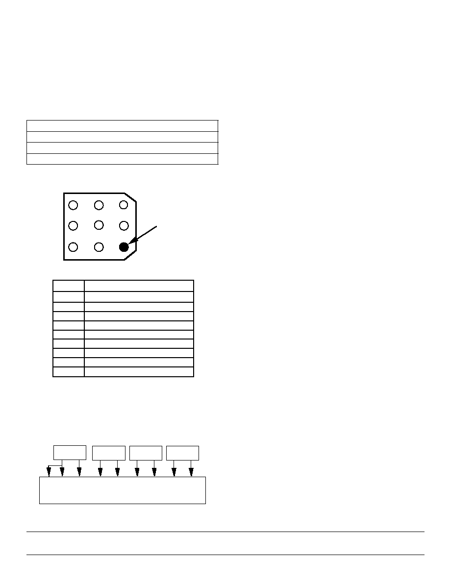
Figure 2 - P1, Power Supply Connector's Pin Assignment
FEMALE
TERMINAL
3
2
1
4
5
6
7
8
9
P1 (top view)
PIN#
1
2
3
4
5
6
7
8
9
PIN ASSIGNMENT
ANALOG - 5.2 V
ANALOG - 5.2 V RETURN # 1 (AGND)
ANALOG - 5.2 V RETURN # 2 (AGND)
ANALOG + 5V
ANALOG + 5 V RETURN (AGND)
DIGITAL - 5.2 V RETURN (DGND)
DIGITAL + 5 V
DIGITAL + 5 V RETURN (DGND)
DIGITAL - 5.2 V
The total power dissipation is typically 1.89 watts, including
the SPT7820 or SPT7824 (1.1 W typ).
POWER SUPPLY HOOK-UPS
Figure 3 - P1 Connector/Hook-Up
P1 POWER CONNECTOR
-5.2 V
+ 5 V
+ 5 V
- 5.2 V
2
3
1
4
5
6
9
7
8
+
-
+
-
+
-
+
-
POWER SUPPLIES AND GROUNDING
The SPT7820/24 requires two analog supply voltages: -
A5.2 V and +A5 V. The +A5 V supply is common to analog
VCC (pin 18 &25) and digital DVCC (pin 14 and 28). A ferrite
bead in series with each supply (RF1 and RF2) reduces the
transient noise injected into VCC. The bead (RF1 or RF2) to
SPT7820/24 connections should not be shared with any
other device. Bypass each power supply pin as closely as
possible to the device (0.1
µ
F to AGND for each VEE and
VCC pin and 0.01
µ
F to DGND for the DVCC pin).
AGND and DGND are isolated on the SPT7820 and SPT7824.
Both -A5.2 V and +A5 V are the analog supply sources. As
in most very high speed ADCs, grounding is critical. There-
fore, the ground plane technique is the most desirable for the
SPT7820/24. To accomplish this, split and tie together the
AGND and DGND ground planesonly at the device (SPT7820/
24) through an RF bead. The EB7820/24 is a four-layer
printed circuit board: the top signal, ground (AGND & DGND)
plane, power plane and the bottom signal. The two ground
planes are connected together at the device through a ferrite
bead (RF3). All three ferrite beads (RF1-3) are located close
to the ADC.
The analog input (pin 21) is physically sandwiched between
the reference taps. Carefully plan printed circuit board layout
to minimize any pick-up from VIN (high frequency) into the
references (VFT or VFB).
REFERENCE CIRCUIT
The SPT7820/24 requires the use of two voltage references:
VFT and VFB. VFT is the force for the top of the voltage
reference ladder (+2.5 V typ), and VFB (-2.5 V typ) is the force
for the bottom of the voltage reference ladder. Both voltages
are applied across an internal reference ladder resistance of
900
. In addition, there are three reference ladder taps:
VST, VRM and VSB. VST is the top of the reference ladder
tap (+2 V), VRM is the middle point (0.0 V typ), and VSB is the
bottom of the reference ladder tap (-2 V). The voltages seen
at VST and VSB are the expected full scale input voltages of
the device when VFT and VFB are driven to the recom-
mended voltages (+2.5 V and -2.5 V respectively). Use VST
and VSB to monitor the actual full scale input voltages (
±
2 V)
by adjusting VFT and VFB. These adjustments have some
interaction; repeat a few times as needed until VST and VSB
settle at the desired voltages. Do not drive VRM as is
commonly done with a standard flash ADC converter. When
not being used (VST, VRM & VSB), decouple with a 0.01
µ
F
chip capacitor (surface mounted) to AGND from each tap to
minimize high frequency noise injection.
Referring to figure 17, U2 is the + 2.5 V reference with
±
150 mV of adjustable range (R1 potentiometer). U3 (OP-
-07) is an inverting amplifier. Its tolerance is 5% with
±
300 mV
of adjustable range (R2 potentiometer). Fairchild recom-

3
5 / 2 2 / 9 7
AN7820/24
frequency. On both devices, the expected full scale analog
input range is from VST to VSB. The analog input is latched
at the leading edge of the CLK. There are 11 digital TTL
outputs. D0 - D9 are the parallel TTL-output bits, with D0 the
LSB, D9 the MSB and D10 the overrange bit. The data
outputs are latched at the rising edge of the CLK, with a
propagation delay of typically 14 nsec. There is one clock
latency between CLK and valid output data (see figure 5 for
more detail). The output code is a straight binary:
Table 3: SPT7820/24 Output Coding
(ÿ Indicates the Flickering Bit Between Logic 0 and 1)
Analog Input
D12 (Overrange Bit) Data Output Code
<- 2.0 V
0
OO OOOO OOOO
- 2.0 V +1 LSB
0
OO OOOO OOOÿ
0 V
0
ÿÿ ÿÿÿÿ ÿÿÿÿ
+ 2.0 V - 1 LSB
0
11 1111 111ÿ
> + 2.0 V + 1/2 LSB
1
11 1111 1111
Pin 21 is the analog input pin. Selecting the analog input
driver for the SPT7820/24 is less of an issue than with most
Flash ADCs because the input impedance and input capaci-
tance are typically 300 k
and 5 pF, respectively. For
example, at 10 MHz and 4 V
P-P
sinewave input, the input
driver source only requires 0.648 mA of peak output current
(4
FC).
The analog input is directly fed from a BNC (VIN). R10 (51
), analog input source termination is mounted on a socket
as a user-selectable termination. The analog input pin has
no circuit protection. Its maximum rating is from VFT to VFB
(
±
2.5 V). In an application in which the analog input range is
greater than
±
2.5 V, protect the input pin from permanent
damage with a voltage limiter.
INPUT CLOCK DRIVER
CLK is the single-ended input clock to the EB7820/24 (evalu-
ation board), CLK IN is the input clock to the SPT7820 or
SPT7824, and CCLK is the capture clock used for the output
latches (U7 & U8).
The clock input of the SPT7820/24 requires a TTL-logic level
of 6 nsec or faster to improve the noise. TTL-logic family
(74FXX) is good for driving the SPT7820/24. Finding a TTL-
square wave generator up to 40 MHz with fast slew rate and
low jitter is harder than a sine wave, low jitter generator. U5
(MAX9686, TTL-voltage comparator) provides most of the
above requirements to drive the SPT7820 or SPT7824 (ex-
cept the low jitter generator). The CLK signal can be a sine
wave signal with the amplitude not to exceed
±
3 V (input
common mode limitation of U5). R11 (51
) is the CLK
source termination. Use R3 to adjust the duty cycle of the
CLK IN. CLK IN is in phase with CLK and has a a propagation
delay of 6 nsec typically. The positive clock (CLK IN) pulse
width must be kept between 10 nsec and 300 nsec for the
mends that these references (VFT & VFB) be operated to
within
±
2% (or
±
2.5 V
±
50 mV) to maintain accuracy within
the specified limit. Before each EB7820/24 board is shipped,
the references are adjusted for VFT and VFB of
±
2.5 V
±
5 mV
respectively. For each new SPT7820 or SPT7824, VST and
VSB need to be readjusted. All measurement must be
referenced to AGND test point (provided).
REFERENCE MONITORING
Table 2 - Recommended Operating Voltage Range
Monitoring
Ref
Point
Min
Typ
Max
Adjust
VST
U1, PIN 20
+1.95 V
+2.00 V +2.05 V
R1
VSB
U1, PIN 23
- 2.05 V
- 2.00 V - 1.95 V
R2
Note that the SPT7820 and SPT7824 (especially refer-
ence taps VFT VFB, VST and VRM) are sensitive to
electrostatic discharge (ESD).
Figure 4A shows one type of reference driver. Figure 4B is
another way to drive the reference circuits using force and
sense. The alternate circuit provides better control of plus
full scale (+FS) and minus full scale (-FS) errors by sensing
VST and VSB to
±
2.0 V respectively. However, the refer-
ence pins VST and VSB are not low impedance nodes that
require additional precaution when routing (PCB layout).
Figure 4A - Reference Driver
REF-03
VFT
VFB
OP-07
+
-
-2.5 V
R
R
Figure 4B - Alternative Reference Driver
10 k
OP-07
+
-
OP-07
+
-
+2.0 V
REF-03
OUT
10 k
10 k
VFT
VST
VSB
VFB
0.1
+2.0 V
-2.0 V
-2.5 V
+2.5 V
+2.5 V
SPT7820 OR SPT7824, 10-BIT ADC
The SPT7820 integrated circuit is a 10-bit analog-to-digital
converter capable of digitizing an input signal with a minimum
update rate of 20 mega-samples per second (MSPS). The
SPT7824, on the other hand is pin compatible with the
SPT7820 except that it is faster: 40 MSPS for the sampling

4
5 / 2 2 / 9 7
AN7820/24
SPT7824 and 20 to 300 nsec for SPT7820. This is due to the
internal THA. When operating the SPT7820 or SPT7824
faster than 3 MSPS, keep the clock duty cycle at approxi-
mately 50%
±
10%. The probe jack PJ1 is the monitoring test
point for the CLK IN. Use this test point when adjusting the
clock duty cycle.
Logic low of the CLK IN (pin 17) causes the internal THA to
go into track. It is necessary to keep the SPT7820 or
SPT7824 in the track mode when the device is idle for an
extended period of time or at the start-up time. This setup will
prevent the internal THA from going to saturation due to the
internal THA's droop. EB7820/24 provides a logic low to the
clock of the SPT7820/24 when the pulse generator (CLK) is
removed from the evaluation board.
TTL-OUTPUT DATA LATCHES
The rise time (Trise) and fall time (Tfall) of SPT7820/24 (D0-
D9) are not symmetrical. The propagation delay with respect
to trise (at the 2.4 V crossing) is typically 14 nsec and 6 nsec
is typical with respect to tfall (at the 2.4 V crossing). Figure
5 shows the actual output characteristic of the SPT7820/24.
This nonsymmetrical trise and tfall creates approximately
8 nsec of invalid data.
In an application where a reconstruction DAC is needed, the
above invalid data zone will cause the reconstruction signal
to have an unwanted heavy glitch if the DAC is directly
interfaced with SPT7820 or SPT7824. To avoid this, buffer
the SPT7820/24 by the edge-triggered latches. FAST family
TTL logic will fit well in this application due to its fast setup and
hold time.
U7 and U8 (74F174) are the output latches. The FAST family
TTL-logic is very sensitive to electrostatic discharge (ESD).
RN1 and RN2 are the 8 pin SIP resistor networks, 10 k
.
They protect U7 and U8 by providing the ESD path to DGND.
The BNC connector (CCLK) is the capture clock, which has
51
termination R12 on board. The outputs of the data
latches (D0-D9) are routed through the standard 26-pin
female ribbon connector (P2). SJ3-5 are the solder jumper
options for the capture clock. Only one of these jumpers
needs to be connected:
-
When SJ3 is installed (factory installed when this board is
shipped), SPT7820/24 and the latches (U7 and U8) are
clocked at the same time. With this configuration, the data
seen at the connector P2 adds another clock of latency
(two clocks of latency total as shown in figure 6).
-
When SJ4 is installed, the capture clock must be supplied
externally through CCLK. The setup time (ts) and hold
time (th) in table 5 must be met when selecting this option.
-
When SJ5 is selected, the buffers will be latched at the
falling edge of the CLK IN (SPT7820/24). With this option,
the setup time (ts) and hold time requirements for the
74F174 latches must be met (table 5). The placement of
this capture clock edge is dependent on the clock pulse
width and the sampling frequency. This option is not
recommended above 25 MSPS to avoid latching the
invalid data.
Figure 5 - Digital Output Characteristic of the SPT7820 or SPT7824
N+1
INVALID
DATA
Rise Time
6nSEC
2.4V
2.4V
Invalid
Data
t
pd1
(14 nS typ.)
6nS
typ.
CLK IN
DATA OUT
(Actual)
N
(N-2)
(N-1)
(N-2)
(N-1)
Invalid
Data
(N)
INVALID
DATA
(N-1)
DATA OUT
(Equivalent)
3.5V
0.8V
0.5V
The digital outputs (latched) are routed through P2, 26 pin ribbon connector. (See table 4.)
The overrange bit (D10) could be viewed through test point TP13. D10 does not bring out through P2.

5
5 / 2 2 / 9 7
AN7820/24
Figure 6 - EB7820/24 Timing Diagram Where CCLK is the Same as CLK IN
Figure 7 - EB7820/24 Timing Diagram Where CCLK is 180
∞
Out of Phase From CLK IN
N
N+1
N+2
N+3
N+4
t
s
VALID
(N-1)
VALID
(N)
VALID
(N+1)
VALID
(N+2)
VALID
(N-2)
(N-1)
(N)
(N+1)
(N-2)
INVALID
INVALID
INVALID
INVALID
t
pd2
t
pd3
t
pd1
t
pwL
t
pwH
t
pd4
t
h
CLK
(EB7820/24)
CLK IN
(
SPT7820/24)
DATA OUT
(SPT7820/24)
CCLK
(LATCHES)
DATA OUT
(P2)
U5, pin 3
Table 4 - P2, SPT7820/24 Output Data (Latched) , 26-Pin Female Ribbon Connector
P2
Function
Logic
P2
Function
Logic
1
CCLK
TTL
2
DGND
DGND
3
N/A
TTL/LO
4
DGND
DGND
5
N/A
TTL/LO
6
DGND
DGND
7
D0 (LSB)
TTL
8
DGND
DGND
9
D1
TTL
10
DGND
DGND
11
D2
TTL
12
DGND
DGND
13
D3
TTL
14
DGND
DGND
15
D4
TTL
16
DGND
DGND
17
D5
TTL
18
DGND
DGND
19
D6
TTL
20
DGND
DGND
21
D7
TTL
22
DGND
DGND
23
D8
TTL
24
DGND
DGND
25
D9 (MSB)
TTL
26
DGND
DGND