 | –≠–ª–µ–∫—Ç—Ä–æ–Ω–Ω—ã–π –∫–æ–º–ø–æ–Ω–µ–Ω—Ç: FDD6676S | –°–∫–∞—á–∞—Ç—å:  PDF PDF  ZIP ZIP |
December 2002
©
2002 Fairchild Semiconductor Corporation
FDD6676S Rev D (W)
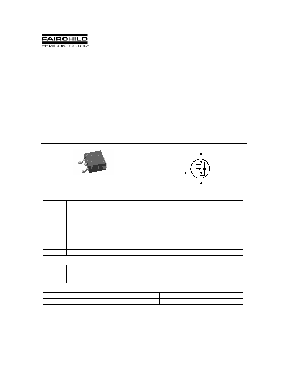
FDD6676S
30V N-Channel PowerTrench
Æ
MOSFET
General Description
The FDS6676S is designed to replace a DPAK
MOSFET and Schottky diode in synchronous DC:DC
power supplies. This 30V MOSFET is designed to
maximize power conversion efficiency, providing a low
R
DS(ON)
and low gate charge. The FDD6676S includes
an integrated Schottky diode using Fairchild's
monolithic SyncFET technology.
Applications
∑
DC/DC converter
Features
∑
78 A, 30 V
R
DS(ON)
= 6.0 m
@ V
GS
= 10 V
R
DS(ON)
= 7.1 m
@ V
GS
= 4.5 V
∑
Low gate charge
∑
Fast Switching
∑
High performance trench technology for extremely
low R
DS(ON)
G
S
D
TO-252
D-PAK
(TO-252)
S
G
D
Absolute Maximum Ratings
T
A
=25
o
C unless otherwise noted
Symbol
Parameter
Ratings
Units
V
DSS
Drain-Source Voltage
30
V
V
GSS
Gate-Source Voltage
±
16
V
I
D
Drain Current ≠ Continuous
(Note 3)
78
A
≠ Pulsed
(Note 1a)
100
Power Dissipation for Single Operation
(Note 1)
70
(Note 1a)
3.1
P
D
(Note 1b)
1.3
W
T
J
, T
STG
Operating and Storage Junction Temperature Range
≠55 to +150
∞
C
Thermal Characteristics
R
JC
Thermal Resistance, Junction-to-Case
(Note 1)
1.8
∞
C/W
R
JA
Thermal Resistance, Junction-to-Ambient
(Note 1a)
40
∞
C/W
R
JA
Thermal Resistance, Junction-to-Ambient
(Note 1b)
96
∞
C/W
Package Marking and Ordering Information
Device Marking
Device
Reel Size
Tape width
Quantity
FDD6676S
FDD6676S
13''
12mm
2500 units
FDD6676S
FDD6676S Rev. D (W)
Electrical Characteristics
T
A
= 25∞C unless otherwise noted
Symbol
Parameter
Test Conditions
Min Typ Max Units
Drain-Source Avalanche Ratings
(Note 2)
W
DSS
Drain-Source Avalanche Energy
Single Pulse, V
DD
= 15 V, I
D
= 16A
250
mJ
I
AR
Drain-Source Avalanche Current
16
A
Off Characteristics
BV
DSS
Drain≠Source Breakdown Voltage V
GS
= 0 V, I
D
= 1 mA
30
V
BV
DSS
T
J
Breakdown Voltage Temperature
Coefficient
I
D
= 10 mA, Referenced to 25
∞
C
24
mV/
∞
C
I
DSS
Zero Gate Voltage Drain Current
V
DS
= 24 V,
V
GS
= 0 V
500
µ
A
I
GSS
Gate≠Body Leakage
V
GS
= ±16 V, V
DS
= 0 V
±100
nA
On Characteristics
(Note 2)
V
GS(th)
Gate Threshold Voltage
V
DS
= V
GS
, I
D
= 1 mA
1
1.3
3
V
V
GS(th)
T
J
Gate Threshold Voltage
Temperature Coefficient
I
D
= 10 mA, Referenced to 25
∞
C
≠0.9
mV/
∞
C
R
DS(on)
Static Drain≠Source
On≠Resistance
V
GS
= 10 V, I
D
= 16 A
V
GS
= 4.5 V, I
D
= 15 A
V
GS
= 10 V, I
D
= 16 A,T
J
=125
∞
C
4.6
5.2
7.2
6.0
7.1
9.0
m
g
FS
Forward Transconductance
V
DS
= 5 V,
I
D
= 16 A
79
S
I
D(on)
On-State Drain Current
V
GS
= 10 V, V
DS
= 5 V
60
A
Dynamic Characteristics
C
iss
Input Capacitance
4770
pF
C
oss
Output Capacitance
840
pF
C
rss
Reverse Transfer Capacitance
V
DS
= 15 V,
V
GS
= 0 V,
f = 1.0 MHz
305
pF
R
G
Gate Resistance
V
GS
= 0 V, f = 1.0 MHz
1.5
Switching Characteristics
(Note 2)
t
d(on)
Turn≠On Delay Time
13
23
ns
t
r
Turn≠On Rise Time
13
23
ns
t
d(off)
Turn≠Off Delay Time
86
138
ns
t
f
Turn≠Off Fall Time
V
DD
= 15 V,
I
D
= 1 A,
V
GS
= 10 V,
R
GEN
= 6
34
54
ns
Q
g
Total Gate Charge
41
58
nC
Q
gs
Gate≠Source Charge
10
nC
Q
gd
Gate≠Drain Charge
V
DS
= 15V,
I
D
= 16 A,
V
GS
= 5 V
10
nC
FDD6676S
FDD6676S Rev. D (W)
D
R
P
DS(ON)
Electrical Characteristics
(continued)
T
A
= 25∞C unless otherwise noted
Symbol
Parameter
Test Conditions
Min Typ Max Units
Drain≠Source Diode Characteristics and Maximum Ratings
I
S
Maximum Continuous Drain≠Source Diode Forward Current
3.5
A
V
SD
Drain≠Source Diode Forward
Voltage
V
GS
= 0 V, I
S
= 3.5 A
(Note 2)
385
700
mV
t
RR
Diode Reverse Recovery Time
29
ns
I
RM
Maximum Recovery Current
2.1
A
Q
RR
Diode Reverse Recovery Charge
dI
F
/dt = 300A/us, I
F
= 16A
30
nC
Notes:
1. R
JA
is the sum of the junction-to-case and case-to-ambient thermal resistance where the case thermal reference is defined as the solder mounting surface of
the drain pins. R
JC
is guaranteed by design while R
CA
is determined by the user's board design.
a) R
JA
= 40∞C/W when mounted on a
1in
2
pad of 2 oz copper
b) R
JA
= 96∞C/W when mounted
on a minimum pad.
Scale 1 : 1 on letter size paper
2. Pulse Test: Pulse Width < 300
µ
s, Duty Cycle < 2.0%
3. Maximum current is calculated as:
where P
D
is maximum power dissipation at T
C
= 25∞C and R
DS(on)
is at T
J(max)
and V
GS
= 10V. Package current limitation is 21A
FDD6676S
FDD6676S Rev. D (W)
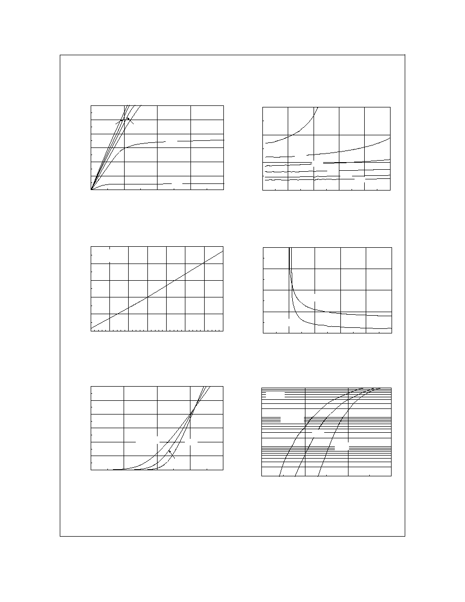
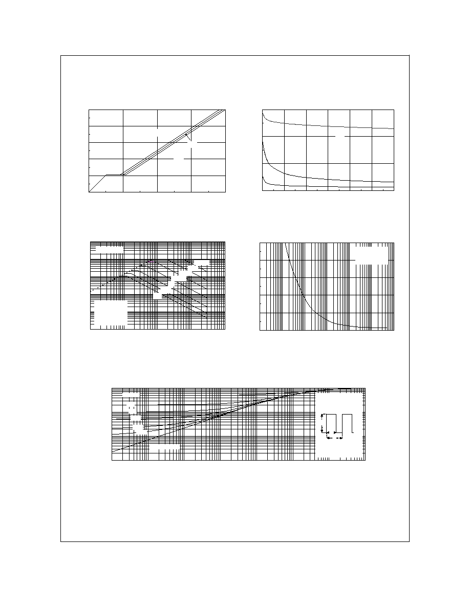
Typical Characteristics
0
15
30
45
60
75
90
0
0.5
1
1.5
2
V
DS
, DRAIN-SOURCE VOLTAGE (V)
I
D
, DRAIN CURRENT (A)
2.5V
4.5V
V
GS
= 10V
2.0V
3.5V
3.0V
0.8
1.3
1.8
2.3
0
20
40
60
80
100
I
D
, DRAIN CURRENT (A)
R
DS(ON)
, NORMALIZED
DRAIN-SOURCE ON-RESISTANCE
V
GS
= 2.5V
6.0V
3.0V
3.5V
10V
4.5V
Figure 1. On-Region Characteristics
Figure 2. On-Resistance Variation with
Drain Current and Gate Voltage
0.6
0.8
1
1.2
1.4
1.6
-50
-25
0
25
50
75
100
125
T
J
, JUNCTION TEMPERATURE (
o
C)
R
DS(ON)
, NORMALIZED
DRAIN-SOURCE ON-RESISTANCE
I
D
= 78A
V
GS
=10V
0.004
0.008
0.012
0.016
0.02
0
2
4
6
8
10
V
GS
, GATE TO SOURCE VOLTAGE (V)
R
DS(ON)
, ON-RESISTANCE (OHM)
I
D
= 8.0A
T
A
= 125
o
C
T
A
=25
o
C
Figure 3. On-Resistance Variation
with Temperature
Figure 4. On-Resistance Variation with
Gate-to-Source Voltage
0
15
30
45
60
75
90
1
1.5
2
2.5
3
V
GS
, GATE TO SOURCE VOLTAGE (V)
I
D
, DRAIN CURRENT (A)
T
A
= 125
o
C
25
o
C
-55
o
C
V
DS
= 5V
0.01
0.1
1
10
0
0.2
0.4
0.6
V
SD
, BODY DIODE FORWARD VOLTAGE (V)
I
S
, REVERSE DRAIN CURRENT (A)
T
A
= 125
o
C
25
o
C
-55
o
C
V
GS
= 0V
Figure 5. Transfer Characteristics
Figure 6. Body Diode Forward Voltage Variation
with Source Current and Temperature
FDD6676S
FDD6676S Rev. D (W)
Typical Characteristics
0
2
4
6
8
10
0
20
40
60
80
Q
g
, GATE CHARGE (nC)
V
GS
, GATE-SOURCE VOLTAGE (V)
I
D
= 78A
V
DS
= 10V
20V
15V
0
2000
4000
6000
0
5
10
15
20
25
30
V
DS
, DRAIN TO SOURCE VOLTAGE (V)
CAPACITANCE (pF)
C
iss
f = 1MHz
V
GS
= 0 V
C
rss
C
oss
Figure 7. Gate Charge Characteristics
Figure 8. Capacitance Characteristics
0.01
0.1
1
10
100
1000
0.01
0.1
1
10
100
V
DS
, DRAIN-SOURCE VOLTAGE (V)
I
D
, DRAIN CURRENT (A)
DC
1s
100ms
R
DS(ON)
LIMIT
V
GS
= 10V
SINGLE PULSE
R
JA
= 125
o
C/W
T
A
= 25
o
C
10ms
10s
100us
1ms
0
10
20
30
40
50
0.001
0.01
0.1
1
10
100
1000
t
1
, TIME (sec)
P(pk), PEAK TRANSIENT POWER (W)
SINGLE PULSE
R
JA
= 125∞C/W
T
A
= 25∞C
Figure 9. Maximum Safe Operating Area
Figure 10. Single Pulse Maximum
Power Dissipation
0.001
0.01
0.1
1
0.0001
0.001
0.01
0.1
1
10
100
1000
t
1
, TIME (sec)
r(t), NORMALIZED EFFECTIVE TRANSIENT
THERMAL RESISTANCE
R
JA
(t) = r(t) * R
JA
R
JA
= 125 ∞C/W
T
J
- T
A
= P * R
JA
(t)
Duty Cycle, D = t
1
/ t
2
P(pk
t
1
t
2
SINGLE PULSE
0.01
0.02
0.05
0.1
0.2
D = 0.5
Figure 11. Transient Thermal Response Curve
Thermal characterization performed using the conditions described in Note 1b.
Transient thermal response will change depending on the circuit board design.
FDD6676S

DISCLAIMER
FAIRCHILD SEMICONDUCTOR RESERVES THE RIGHT TO MAKE CHANGES WITHOUT FURTHER
NOTICE TO ANY PRODUCTS HEREIN TO IMPROVE RELIABILITY, FUNCTION OR DESIGN. FAIRCHILD
DOES NOT ASSUME ANY LIABILITY ARISING OUT OF THE APPLICATION OR USE OF ANY PRODUCT
OR CIRCUIT DESCRIBED HEREIN; NEITHER DOES IT CONVEY ANY LICENSE UNDER ITS PATENT
RIGHTS, NOR THE RIGHTS OF OTHERS.
TRADEMARKS
The following are registered and unregistered trademarks Fairchild Semiconductor owns or is authorized to use and is
not intended to be an exhaustive list of all such trademarks.
LIFE SUPPORT POLICY
FAIRCHILDS PRODUCTS ARE NOT AUTHORIZED FOR USE AS CRITICAL COMPONENTS IN LIFE SUPPORT
DEVICES OR SYSTEMS WITHOUT THE EXPRESS WRITTEN APPROVAL OF FAIRCHILD SEMICONDUCTOR CORPORATION.
As used herein:
1. Life support devices or systems are devices or
systems which, (a) are intended for surgical implant into
the body, or (b) support or sustain life, or (c) whose
failure to perform when properly used in accordance
with instructions for use provided in the labeling, can be
reasonably expected to result in significant injury to the
user.
2. A critical component is any component of a life
support device or system whose failure to perform can
be reasonably expected to cause the failure of the life
support device or system, or to affect its safety or
effectiveness.
PRODUCT STATUS DEFINITIONS
Definition of Terms
Datasheet Identification
Product Status
Definition
Advance Information
Preliminary
No Identification Needed
Obsolete
This datasheet contains the design specifications for
product development. Specifications may change in
any manner without notice.
This datasheet contains preliminary data, and
supplementary data will be published at a later date.
Fairchild Semiconductor reserves the right to make
changes at any time without notice in order to improve
design.
This datasheet contains final specifications. Fairchild
Semiconductor reserves the right to make changes at
any time without notice in order to improve design.
This datasheet contains specifications on a product
that has been discontinued by Fairchild semiconductor.
The datasheet is printed for reference information only.
Formative or
In Design
First Production
Full Production
Not In Production
ImpliedDisconnect
ISOPLANAR
LittleFET
MicroFET
MicroPak
MICROWIRE
MSX
MSXPro
OCX
OCXPro
OPTOLOGIC
‚
OPTOPLANAR
FACT
FACT Quiet Series
FAST
‚
FASTr
FRFET
GlobalOptoisolator
GTO
HiSeC
I
2
C
Rev. I1
ACEx
ActiveArray
Bottomless
CoolFET
CROSSVOLT
DOME
EcoSPARK
E
2
CMOS
TM
EnSigna
TM
PACMAN
POP
Power247
PowerTrench
‚
QFET
QS
QT Optoelectronics
Quiet Series
RapidConfigure
RapidConnect
SILENT SWITCHER
‚
SMART START
SPM
Stealth
SuperSOT-3
SuperSOT-6
SuperSOT-8
SyncFET
TinyLogic
TruTranslation
UHC
UltraFET
‚
VCX
Across the board. Around the world.
The Power Franchise
Programmable Active Droop