
July 1998
FSB619
NPN Low Saturation Transistor
These devices are designed with high current gain and low saturation voltage with collector currents up to 3A
continuous.
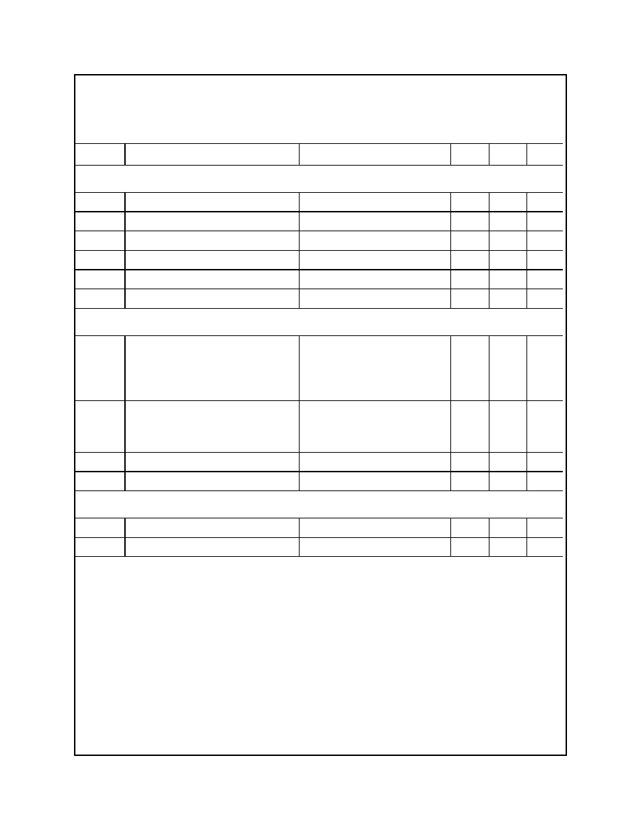
Absolute Maximum Ratings*
T
A = 25įC unless otherwise noted
įC
-55 to +150
Operating and Storage Junction Temperature Range
T
J,
T
stg
A
2
Collector Current - Continuous
I
C
V
5
Emitter-Base Voltage
V
EBO
V
50
Collector-Base Voltage
V
CBO
V
50
Collector-Emitter Voltage
V
CEO
Units
FSB619
Parameter
Symbol
*These ratings are limiting values above which the serviceability of any semiconductor device may be impaired.
NOTES:
1) These ratings are based on a maximum junction temperature of 150įC.
2) These are steady state limits. The factory should be consulted on applications involving pulsed or low duty cycle operations.
Thermal Characteristics
T
A = 25įC unless otherwise noted
įC/W
250
Thermal Resistance, Junction to Ambient
R
JA
mW
mW/įC
500
4
Total Device Dissipation*
Derate above 25įC
P
D
FSB619
Units
Max
Characteristic
Symbol
Page 1 of 2
FSB619
Discrete Power & Signal
Technologies
©
1998 Fairchild Semiconductor Corporation
SuperSOT
TM
-3 (SOT-23)
C
E
B
*Device mounted on FR-4 PCB 4.5" X 5"; mounting pad 0.02 in
2
of 2oz copper.
-
100
I
C
= 50 mA,V
CE
= 10 V, f=100MHz
Transition Frequency
f
T
pF
30
V
CB
= 10 V, I
E
= 0, f = 1MHz
Output Capacitance
C
obo
SMALL SIGNAL CHARACTERISTICS
V
1
I
C
= 2 A, V
CE
= 2 V
Base-Emitter On Voltage
V
BE(on)
V
1
I
C
= 2 A, I
B
= 50 mA
Base-Emitter Saturation Voltage
V
BE(sat)
mV
20
235
320
I
C
= 100 mA, I
B
= 10 mA
I
C
= 1 A, I
B
= 10 mA
I
C
= 2 A, I
B
= 50 mA
Collector-Emitter Saturation Voltage
V
CE(sat)
-
200
300
200
100
I
C
= 10 mA, V
CE
= 2V
I
C
= 200 mA, V
CE
= 2V
I
C
= 1A, V
CE
= 2V
I
C
= 2A, V
CE
= 2V
DC Current Gain
h
FE
ON CHARACTERISTICS*
nA
100
V
CES
= 40 V
Collector Emitter Cutoff Current
I
CES
nA
100
V
EB
= 4V
Emitter Cutoff Current
I
EBO
nA
100
V
CB
= 40 V
Collector Cutoff Current
I
CBO
V
5
I
E
= 100
Ķ
A
Emitter-Base Breakdown Voltage
BV
EBO
V
50
I
C
= 100
Ķ
A
Collector-Base Breakdown Voltage
BV
CBO
V
50
I
C
= 10 mA
Collector-Emitter Breakdown Voltage
BV
CEO
OFF CHARACTERISTICS
Units
Max
Min
Test Conditions
Parameter
Symbol
NPN Low Saturation Transistor
(continued)
Electrical Characteristics
T
A = 25įC unless otherwise noted
*Pulse Test: Pulse Width
300
Ķ
s, Duty Cycle
2.0%
Page 2 of 2
FSB619
fsb619.lwpPrNA 7/10/98 revC