 | ÐлекÑÑоннÑй компоненÑ: IRF610 | СкаÑаÑÑ:  PDF PDF  ZIP ZIP |
IRF610 3.3A, 200V, 1.500 Ohm, N-Channel Power MOSFET
©2002 Fairchild Semiconductor Corporation
IRF610 Rev. B
IRF610
3.3A, 200V, 1.500 Ohm, N-Channel Power
MOSFET
This N-Channel enhancement mode silicon gate power field
effect transistor is an advanced power MOSFET designed,
tested, and guaranteed to withstand a specified level of
energy in the breakdown avalanche mode of operation. All of
these power MOSFETs are designed for applications such
as switching regulators, switching convertors, motor drivers,
relay drivers, and drivers for high power bipolar switching
transistors requiring high speed and low gate drive power.
These types can be operated directly from integrated
circuits.
Formerly developmental type TA17442.
Features
· 3.3A, 200V
· r
DS(ON)
= 1.500
· Single Pulse Avalanche Energy Rated
· SOA is Power Dissipation Limited
· Nanosecond Switching Speeds
· Linear Transfer Characteristics
· High Input Impedance
· Related Literature
- TB334 "Guidelines for Soldering Surface Mount
Components to PC Boards"
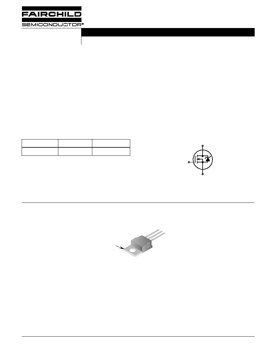
Symbol
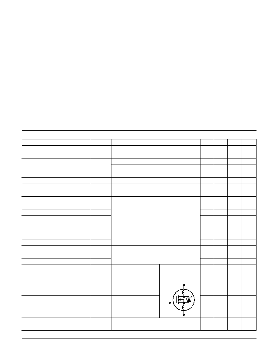
Packaging
JEDEC TO-220AB
Ordering Information
PART NUMBER
PACKAGE
BRAND
IRF610
TO-220AB
IRF610
NOTE: When ordering, use the entire part number.
G
D
S
GATE
DRAIN (FLANGE)
SOURCE
DRAIN
Data Sheet
January 2002
©2002 Fairchild Semiconductor Corporation
IRF610 Rev. B
Absolute Maximum Ratings
T
C
= 25
o
C, Unless Otherwise Specified
IRF610
UNITS
Drain to Source Voltage (Note 1) . . . . . . . . . . . . . . . . . . . . . . . . . . . . . . . . . . . . . . . . . . . . . . V
DS
200
V
Drain to Gate Voltage (R
GS
= 20k
)
(Note 1) . . . . . . . . . . . . . . . . . . . . . . . . . . . . . . . . . . . V
DGR
200
V
Continuous Drain Current . . . . . . . . . . . . . . . . . . . . . . . . . . . . . . . . . . . . . . . . . . . . . . . . . . . . . I
D
T
C
= 100
o
C . . . . . . . . . . . . . . . . . . . . . . . . . . . . . . . . . . . . . . . . . . . . . . . . . . . . . . . . . . . . . . I
D
3.3
2.1
A
A
Pulsed Drain Current (Note 2) . . . . . . . . . . . . . . . . . . . . . . . . . . . . . . . . . . . . . . . . . . . . . . . . . I
DM
8
A
Gate to Source Voltage . . . . . . . . . . . . . . . . . . . . . . . . . . . . . . . . . . . . . . . . . . . . . . . . . . . . . V
GS
±
20
V
Maximum Power Dissipation . . . . . . . . . . . . . . . . . . . . . . . . . . . . . . . . . . . . . . . . . . . . . . . . . . P
D
43
W
Linear Derating Factor . . . . . . . . . . . . . . . . . . . . . . . . . . . . . . . . . . . . . . . . . . . . . . . . . . . . . . . .
0.34
W/
o
C
Single Pulse Avalanche Energy Rating (Note 4) . . . . . . . . . . . . . . . . . . . . . . . . . . . . . . . . . . E
AS
46
mJ
Operating and Storage Temperature . . . . . . . . . . . . . . . . . . . . . . . . . . . . . . . . . . . . . . . .T
J,
T
STG
-55 to 150
o
C
Maximum Temperature for Soldering
Leads at 0.063in (1.6mm) from Case for 10s . . . . . . . . . . . . . . . . . . . . . . . . . . . . . . . . . . . . . T
L
Package Body for 10s, See Techbrief 334 . . . . . . . . . . . . . . . . . . . . . . . . . . . . . . . . . . . . . T
pkg
300
260
o
C
o
C
CAUTION: Stresses above those listed in "Absolute Maximum Ratings" may cause permanent damage to the device. This is a stress only rating and operation of the
device at these or any other conditions above those indicated in the operational sections of this specification is not implied.
NOTE:
1. T
J
= 25
o
C to 125
o
C.
Electrical Specifications
T
C
= 25
o
C, Unless Otherwise Specified
PARAMETER
SYMBOL
TEST CONDITIONS
MIN
TYP
MAX
UNITS
Drain to Source Breakdown Voltage
BV
DSS
V
GS
= 0V, I
D
= 250
µ
A (Figure 10)
200
-
-
V
Gate Threshold Voltage
V
GS(TH)
V
DS
= V
GS
, I
D
= 250
µ
A
2
-
4
V
Zero Gate Voltage Drain Current
I
DSS
V
DS
= Max Rating, V
GS
= 0V
-
-
25
µ
A
V
DS
= Max Rating x 0.8, V
GS
= 0V, T
J
= 125
o
C
-
-
250
µ
A
On-State Drain Current (Note 2)
I
D(ON)
V
DS
> I
D(ON)
x r
DS(ON)MAX
, V
GS
= 10V (Figure 7)
3.3
-
-
A
Gate to Source Leakage Current
I
GSS
V
GS
=
±
20V
-
-
±
100
nA
Drain to Source On Resistance (Note 2)
r
DS(ON)
V
GS
= 10V, I
D
= 1.6A (Figures 8, 9)
-
1.0
1.5
Forward Transconductance (Note 2)
g
fs
V
DS
50V, I
D
= 1.6A (Figure 12)
0.8
1.3
-
S
Turn-On Delay Time
t
d(ON)
V
DD
= 100V, I
D
3.3A, R
G
= 24
, R
L
= 30
MOSFET Switching Times are
Essentially Independent of Operating
Temperature
-
8
12
ns
Rise Time
t
r
-
17
26
ns
Turn-Off Delay Time
t
d(OFF)
-
13
21
ns
Fall Time
t
f
-
9
13
ns
Total Gate Charge
(Gate to Source + Gate to Drain)
Q
g(TOT)
V
GS
= 10V, I
D
= 3.3A, V
DS
= 0.8 x Rated BV
DSS
,
I
g(REF)
= 1.5mA (Figure 14) Gate Charge is
Essentially Independent of Operating
Temperature
-
5.3
8.2
nC
Gate to Source Charge
Q
gs
-
1.2
-
nC
Gate to Drain "Miller" Charge
Q
gd
-
3.0
-
nC
Input Capacitance
C
ISS
V
GS
= 0V, V
DS
= 25V, f = 1MHz
(Figure 11)
-
135
-
pF
Output Capacitance
C
OSS
-
60
-
pF
Reverse Transfer Capacitance
C
RSS
-
16
-
pF
Internal Drain Inductance
L
D
Measured From the
Contact Screw on Tab to
Center of Die
Modified MOSFET
Symbol Showing the
Internal Device
Inductances
-
3.5
-
nH
Measured From the Drain
Lead, 6mm (0.25in) From
Package to Center of Die
-
4.5
-
nH
Internal Source Inductance
L
S
Measured From the Source
Lead, 6mm (0.25in) from
Header to Source Bonding
Pad
-
7.5
-
nH
Thermal Resistance Junction to Case
R
JC
-
-
2.9
o
C/W
Thermal Resistance Junction to Ambient
R
JA
Free Air Operation
-
-
80
o
C/W
L
S
L
D
G
D
S
IRF610
©2002 Fairchild Semiconductor Corporation
IRF610 Rev. B
Source to Drain Diode Specifications
PARAMETER
SYMBOL
TEST CONDITIONS
MIN
TYP
MAX
UNITS
Continuous Source to Drain Current
I
SD
Modified MOSFET Symbol
Showing the Integral
Reverse P-N Junction
Rectifier
-
-
3.3
A
Pulse Source to Drain Current
(Note 3)
I
SDM
-
-
8
A
Source to Drain Diode Voltage (Note 2)
V
SD
T
J
= 25
o
C, I
SD
= 3.3A, V
GS
= 0V (Figure 13)
-
-
2.0
V
Reverse Recovery Time
t
rr
T
J
= 25
o
C, I
SD
= 3.3A, dI
SD
/dt = 100A/
µ
s
75
160
310
ns
Reverse Recovery Charge
Q
RR
T
J
= 25
o
C, I
SD
= 3.3A, dI
SD
/dt = 100A/
µ
s
0.33
0.9
1.4
µ
C
NOTES:
2. Pulse test: pulse width
300
µ
s, duty cycle
2%.
3. Repetitive rating: pulse width limited by maximum junction temperature. See Transient Thermal Impedance curve (Figure 3).
4. V
DD
= 50V, starting T
J
= 25
o
C, L = 6.4mH, R
G
= 25
,
peak I
AS
= 3.3A.
Typical Performance Curves
Unless Otherwise Specified
FIGURE 1. NORMALIZED POWER DISSIPATION vs CASE
TEMPERATURE
FIGURE 2. MAXIMUM CONTINUOUS DRAIN CURRENT vs
CASE TEMPERATURE
FIGURE 3. MAXIMUM TRANSIENT THERMAL IMPEDANCE
G
D
S
0
50
100
150
0
T
C
, CASE TEMPERATURE (
o
C)
PO
WER DISSIP
A
TION MUL
TIPLIER
0.2
0.4
0.6
0.8
1.0
1.2
2.0
1.0
0
25
50
75
100
125
150
4.0
I
D
,
DRAIN CURRENT (A)
T
C
, CASE TEMPERATURE (
o
C)
5.0
3.0
10
1
0.1
0.01
10
-5
10
-4
10
-3
10
-2
0.1
1
10
Z
JC
,
TRANSIENT
THERMAL IMPED
ANCE (
o
C/W)
t
1
, RECTANGULAR PULSE DURATION (S)
SINGLE PULSE
0.1
0.02
0.2
0.5
0.01
0.05
P
DM
NOTES:
DUTY FACTOR: D = t
1
/t
2
PEAK T
J
= P
DM
x Z
JC
+ T
C
t
1
t
2
IRF610
©2002 Fairchild Semiconductor Corporation
IRF610 Rev. B
FIGURE 4. FORWARD BIAS SAFE OPERATING AREA
FIGURE 5. OUTPUT CHARACTERISTICS
FIGURE 6. SATURATION CHARACTERISTICS
FIGURE 7. TRANSFER CHARACTERISTICS
FIGURE 8. DRAIN TO SOURCE ON RESISTANCE vs GATE
VOLTAGE AND DRAIN CURRENT
FIGURE 9. NORMALIZED DRAIN TO SOURCE ON
RESISTANCE vs JUNCTION TEMPERATURE
Typical Performance Curves
Unless Otherwise Specified (Continued)
V
DS
, DRAIN TO SOURCE VOLTAGE (V)
10
0.1
10
1
I
D
,
DRAIN CURRENT (A)
100
100
DC
100
µs
10ms
1
1000
T
J
= 150
o
C SINGLE PULSE
T
C
= 25
o
C
10
µs
1ms
LIMITED BY r
DS(ON)
AREA MAY BE
OPERATION IN THIS
V
DS
, DRAIN TO SOURCE VOLTAGE (V)
I
D
,
DRAIN CURRENT (A)
0
0
20
40
60
80
1
2
3
4
5
100
V
GS
= 10V
V
GS
= 7V
V
GS
= 8V
V
GS
= 6V
V
GS
= 5V
V
GS
= 4V
PULSE DURATION = 80
µs
DUTY CYCLE = 0.5% MAX
0
1
0
2
4
6
10
2
3
I
D
,
DRAIN CURRENT (A)
V
DS
, DRAIN TO SOURCE VOLTAGE (V)
4
8
5
V
GS
= 5V
V
GS
= 10V
V
GS
= 8V
V
GS
= 7V
V
GS
= 6V
V
GS
= 4V
PULSE DURATION = 80
µs
DUTY CYCLE = 0.5% MAX
0
2
4
6
8
10
T
J
= 150
o
C
T
J
= 25
o
C
10
1
0.1
10
-2
V
GS
, GATE TO SOURCE VOLTAGE (V)
I
D
,
DRAIN CURRENT (A)
PULSE DURATION = 80
µs
DUTY CYCLE = 0.5% MAX
V
DS
50V
r
DS(ON),
ON ST
A
TE RESIST
ANCE (
)
15
12
9
6
3
0
0
2
4
6
8
10
I
D
, DRAIN CURRENT (A)
V
GS
= 10V
V
GS
= 20V
PULSE DURATION = 80
µs
DUTY CYCLE = 0.5% MAX
3.0
2.4
1.8
1.2
0.6
0
-60
-40
-20
0
20
40
60
80
100
120 140 160
NORMALIZED DRAIN
T
O
SOURCE
T
J
, JUNCTION TEMPERATURE (
o
C)
ON RESIST
ANCE
PULSE DURATION = 80
µs
DUTY CYCLE = 0.5% MAX
V
GS
= 10V, I
D
= 3.2A
IRF610
©2002 Fairchild Semiconductor Corporation
IRF610 Rev. B
FIGURE 10. NORMALIZED DRAIN TO SOURCE BREAKDOWN
VOLTAGE vs JUNCTION TEMPERATURE
FIGURE 11. CAPACITANCE vs DRAIN TO SOURCE VOLTAGE
FIGURE 12. TRANSCONDUCTANCE vs DRAIN CURRENT
FIGURE 13. SOURCE TO DRAIN DIODE VOLTAGE
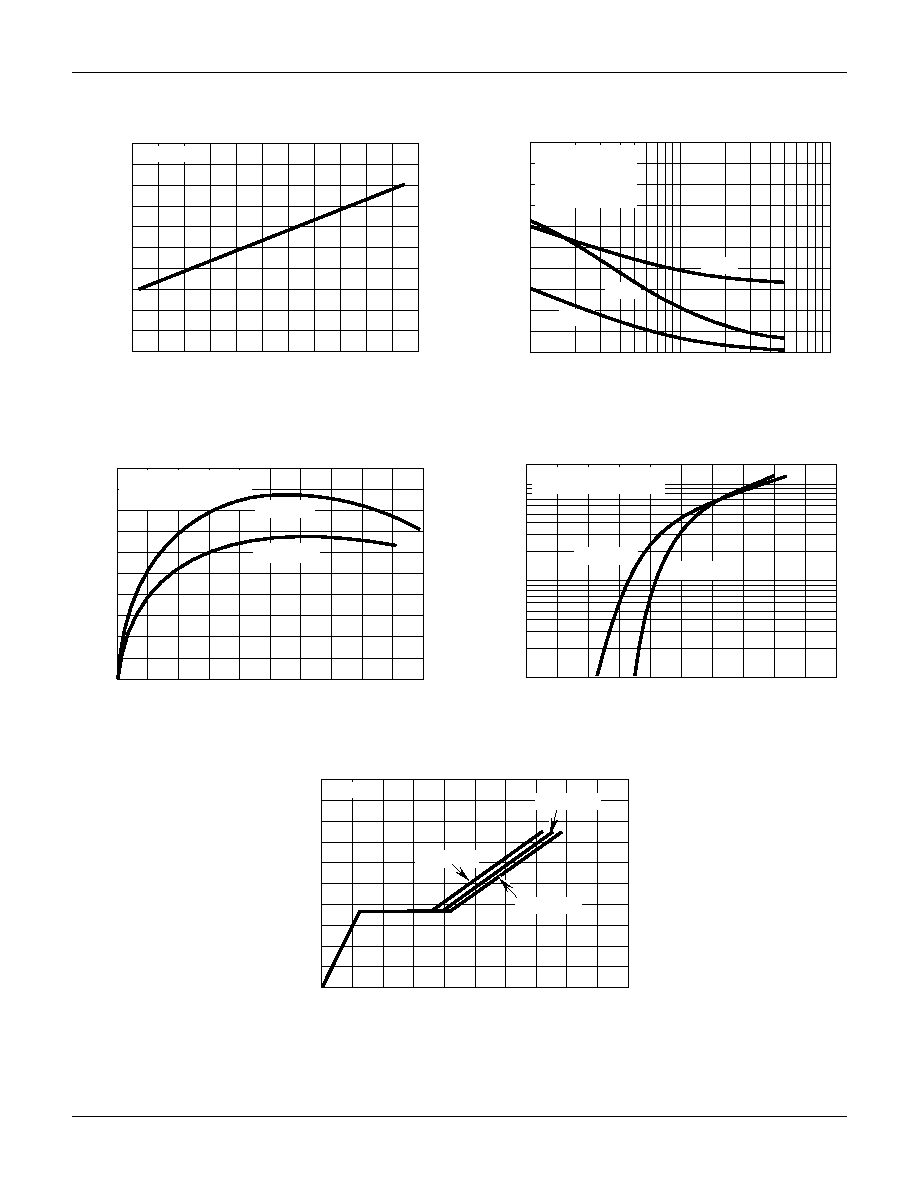
FIGURE 14. GATE TO SOURCE VOLTAGE vs GATE CHARGE
Typical Performance Curves
Unless Otherwise Specified (Continued)
1.25
1.15
1.05
0.95
0.85
0.75
-60
-40
-20
0
20
40
60
80
100 120 140 160
T
J
, JUNCTION TEMPERATURE (
o
C)
NORMALIZED DRAIN
T
O
SOURCE
BREAKDO
WN V
O
L
T
A
G
E
I
D
= 250
µA
400
320
240
160
80
0
1
2
5
10
2
5
10
2
C,
CAP
A
CIT
ANCE (pF)
V
DS
, DRAIN TO SOURCE VOLTAGE (V)
C
OSS
C
RSS
C
ISS
V
GS
= 0V, f = 1MHz
C
RSS
= C
GD
C
OSS
= C
DS
+ C
GD
C
ISS
= C
GS
+ C
GD
1.5
1.2
0.9
0.6
0.3
0
0
1
2
3
4
5
g
fs
,
TRANSCONDUCT
ANCE
(S)
I
D
, DRAIN CURRENT (A)
PULSE DURATION = 80
µs
DUTY CYCLE = 0.5% MAX
V
DS
50V
T
J
= 25
o
C
T
J
= 150
o
C
0
0.8
1.2
0.4
1
10
100
I
SD
,
SOURCE
T
O
DRAIN CURRENT (A)
V
SD
, SOURCE TO DRAIN VOLTAGE (V)
1.6
2.0
T
J
= 25
o
C
T
J
= 150
o
C
PULSE DURATION = 80
µs
DUTY CYCLE = 0.5% MAX
Q
g
, GATE CHARGE (nC)
V
GS
,
GA
TE
T
O
SOURCE
V
O
L
T
A
GE (V)
0
0
2
4
6
8
4
8
12
10
V
DS
= 40V
V
DS
= 160V
V
DS
= 100V
20
16
I
D
= 3.2A
IRF610