 | –≠–ª–µ–∫—Ç—Ä–æ–Ω–Ω—ã–π –∫–æ–º–ø–æ–Ω–µ–Ω—Ç: KA78R12 | –°–∫–∞—á–∞—Ç—å:  PDF PDF  ZIP ZIP |
©2001 Fairchild Semiconductor Corporation
www.fairchildsemi.com
Rev. 1.0.1
Features
∑ 1A / 12V Output low dropout voltage regulator
∑ TO220 Full-Mold package (4PIN)
∑ Overcurrent protection, Thermal shutdown
∑ Overvoltage protection, Short-Circuit protection
∑ With output disable function
Description
The KA78R12 is a low-dropout voltage regulator suitable
for various electronic equipments. It provides constant volt-
age power source with TO-220 4 lead full mold package.
Dropout voltage of KA78R12 is below 0.5V in full rated
current(1A). This regulator has various function such as
peak current protection, thermal shut down, overvoltage pro-
tection and output disable function.
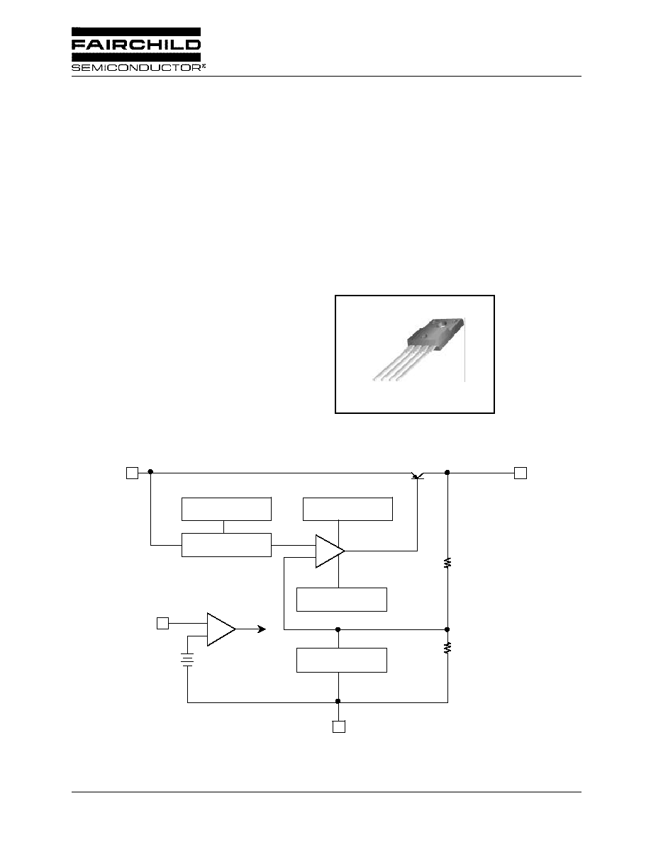
TO-220F-4L
1. Vin 2. Vo 3. GND 4. Vdis
1
Internal Block Diagram
THERMAL SHUTDOWN
BANDGAP REFERENCE
OVERVOLTAGE
PROTECTION
SOA PROTECTION
SHORTCIRCUIT
PROTECTION
1
4
3
2
Vin
Vdis
Vo
GND
HIGH / LOW
OUTPUT
ON / OFF
Q1
R1
R2
-
+
-
+
1.4V
SHORT-CIRCUIT
KA78R12
Low Dropout Voltage Regulator
KA78R12
2
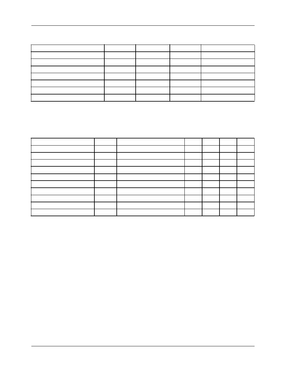
Absolute Maximum Ratings
Electrical Characteristics
(Vin =15V, Io = 0.5A, Ta = 25
∞
C , unless otherwise specified)
Note:
1.These parameters, although guaranteed, are not 100% tested in production.
Parameter
Symbol
Value
Unit
Remark
Input Voltage
Vin
35
V
-
Disable Voltage
Vdis
35
V
-
Output Current
Io
1.0
A
-
Power Dissipation 1
Pd1
1.5
W
No Heatsink
Power Dissipation 2
Pd2
15
W
With Heatsink
Junction Temperature
Tj
+150
∞
C
-
Operating Temperature
Topr
-20 ~ +80
∞
C
-
Parameter
Symbol
Conditions
Min.
Typ.
Max.
Unit
Output Voltage
Vo
-
11.7
12
12.3
V
Load Regulation
Rload
5mA < Io < 1A
-
0.1
2.0
%
Line Regulation
Rline
13V < Vin < 29V
-
0.5
2.5
%
Ripple Rejection Ratio
RR
note1
45
55
-
dB
Dropout Voltage
Vdrop
Io = 1A
-
-
0.5
V
Disable Voltage High
VdisH
Output Active
2.0
-
-
V
Disable Voltage Low
VdisL
Output Disabled
-
-
0.8
V
Disable Bias Current High
IdisH
Vdis = 2.7V
-
-
20
µ
A
Disable Bias Current Low
IdisL
Vdis = 0.4V
-
-
-0.4
mA
Quiescent Current
Iq
Io = 0A
-
-
10
mA

KA78R12
3
Typical Perfomance Characteristics
Figure 1.Output Voltage vs. Input Voltage
Figure 3.Output Voltage vs. Disable Voltage
Figure 5.Quiescent Current vs. Temperature(Tj)
Figure 2.Quiescent Current vs. Input Voltage
Figure 4.Output Voltage vs. Temperature(Tj)
Figure 6.Dropout Voltage vs. Junction Temperature
5
10
15
Input voltage Vin (V)
15.0
12.5
10.0
7.5
5.0
2.5
17.5
0
0
Output voltage
Vo
(V)
RL=
RL=12
20
25
8
0
Output voltage
Vo
(V)
3
Disable voltage Vdis (V)
0.5
1.5
1
2
2.5
15.0
12.5
10.0
7.5
5.0
2.5
17.5
0
10
8
6
4
2
0
Quescent
current
Iq
(
mA
)
Junction temperature Tj(
o
C)
75
125
0
25
50
100
-25
i
50
40
30
20
10
0
0
Quescent
current
Iq
(
mA
)
Input voltage Vin (V)
RL=
5
10
15
20
25
8
i
12.04
12.02
12.00
12.06
-25
Output voltage
Vo
(V)
TEMPERATURE Tj(
o
C)
75
125
0
25
50
100
11.96
11.94
11.92
11.98
125
0.6
0.5
0.4
0.3
0
Dropout voltage
Vdrop
(V)
Junction temperature Tj(
o
C)
0.2
0.1
75
0
25
50
100
-25
Io=1A
0.75A
0.5A
0.25A

KA78R12
4
Typical Perfomance Characteristics (continued)
Figure 7.Power Dissipation vs. Temperature(Ta)
Figure 8. Overcurrent Protection Characteristics
(Typical Value)
-25
Power dissipation P
D
(W)
TEMPERATURE TJ(
o
C)
75
125
0
25
50
100
15
10
5
20
0
D
a
Output Current(A)
Relative output voltage(%)
1.5
2.5
0
0.5
1.0
2.0
80
60
20
100
0
40
3.0
Output Current(A)
Relative output voltage(%)
1.5
2.5
0
0.5
1.0
2.0
80
60
20
100
0
40
3.0
Relative output voltage(%)
1.5
2.5
0
0.5
1.0
2.0
80
60
20
100
0
40
3.0
KA78R12
5
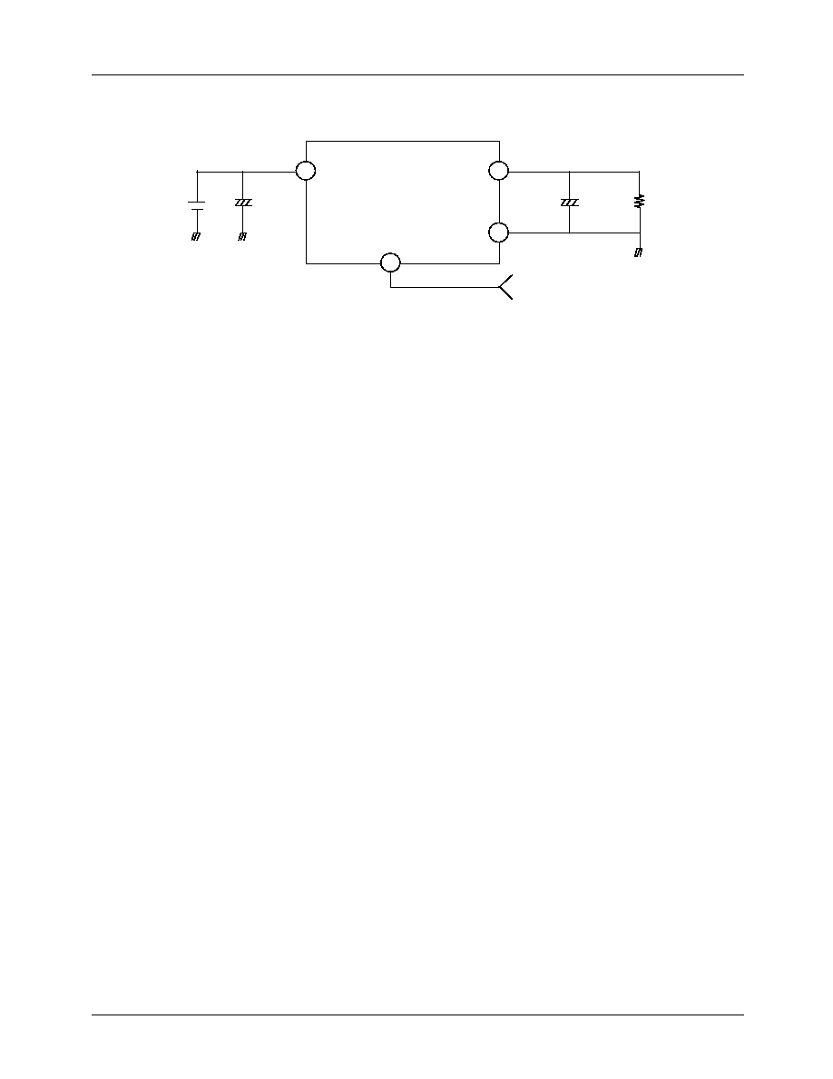
Typical Application
Figure 1.Application Circuit
∑ Ci is required if regulator is located an appreciable distance from power supply filter.
∑ Co improves stability and transient response.(Co > 47
µ
F)
+
+
1
2
3
4
Vin
Vdis
Vo
GND
Disable Signal