 | ÐлекÑÑоннÑй компоненÑ: LM2931A | СкаÑаÑÑ:  PDF PDF  ZIP ZIP |
Äîêóìåíòàöèÿ è îïèñàíèÿ www.docs.chipfind.ru
©2001 Fairchild Semiconductor Corporation
www.fairchildsemi.com
Rev. 1.0.0
Features
· Limited input voltage and high efficiency.
· Internal thermal over load protection.
· 60V load dump protection.
· Output current up to 0.1A.
Description
LM2931A is a fixed 3-terminal low dropout voltage
regulator designed to need very low quiescent current.
Internally, implemented circuits include 60V load dump
protection, -50V reverse transient short circuit and thermal
over load protection.
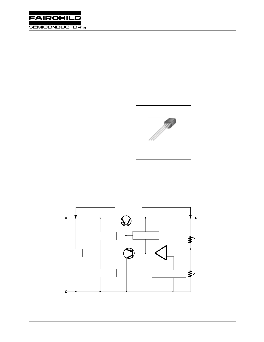
TO-92
1: Output 2: GND 3: Input
1
Internal Block Diagram
0.6V MAX DROP
V
O
V
I
3
2
1
GND
_
+
THERMAL SHUTDOWN
START
OVER VOLTAGE
PROTECTION
CURRENT LIMIT
REFERENCE VOLTAGE
PASS ELEMENT
Input
Output
LM2931A
Low Dropout Voltage Regulator
LM2931A
2
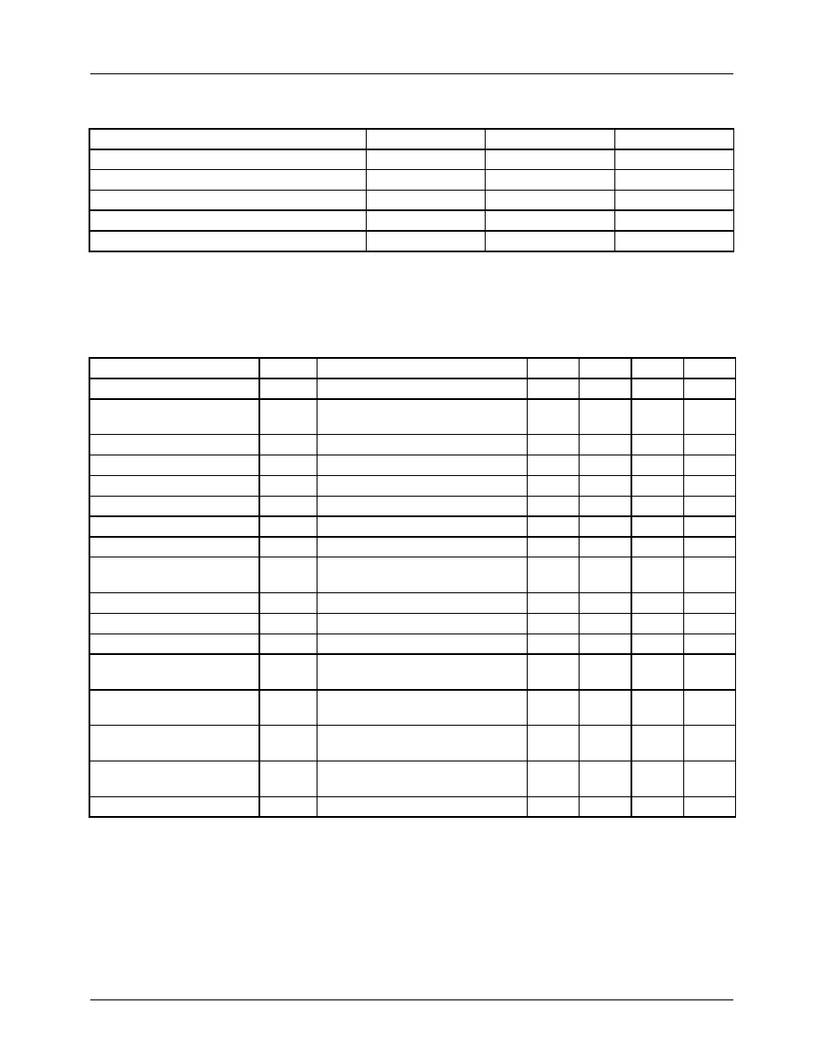
Absolute Maximum Ratings
Electrical Characteristics
(V
I
=14V, I
O
=10mA, C
O
=100
µ
F, T
A
=
25
o
C)
Parameter
Symbol
Value
Unit
Input Voltage
Vi
33
V
Over Protection Voltage
V
(OP)
60
V
Operating Temperature Range
T
OPR
-40~+125
°
C
Maximum Junction Temperature
T
J
150
°
C
Storage Temperature Range
T
STG
-65~+150
°
C
Parameter
Symbol
Conditions
Min.
Typ.
Max.
Unit
Output Voltage (I)
V
O
(I)
V
I
= 14V, I
O
= 10mA
4.81
5.0
5.19
V
Output Voltage (II)
V
O
(II)
V
I
= 6 ~ 26V, I
O
= 100mA
T
J
= -40 ~ +125
o
C
4.75
5.0
5.25
V
Line Regulation (I)
V
O
(I)
V
I
= 9 ~ 16V, I
O
= 10mA
-
2.0
10
mV
Line Regulation (II)
V
O
(II)
V
I
= 6 ~ 26V, I
O
= 10mA
-
4.0
30
mV
Load Regulation
V
O
(III) V
I
= 14V, I
O
= 5 ~ 100mA
-
10
50
mV
Output Impedance
Z
O
V
I
= 14V, I
O
= 100mA
-
100
600
m
Quiescent Current (I)
I
Q
(I)
V
I
= 6 ~ 26V, I
O
10mA
-
0.1
1.0
mA
Quiescent Current (II)
I
Q
(II)
V
I
= 14V, I
O
100mA
-
5.0
30
mA
Output Noise Voltage
V
N
V
I
= 14V, I
O
= 10mA,
f = 10Hz ~ 100KHz
-
150
1000
µ
Vrms
Ripple Rejection
RR
V
I
= 14V, I
O
= 10mA, f = 120Hz
55
80
-
dB
Dropout Voltage (I)
V
D
(I)
I
O
= 10mA, V
D
= V
I
- V
O
-
0.03
0.2
V
Dropout Voltage (II)
V
D
(II)
I
O
= 100mA, V
D
= V
I
- V
O
-
0.1
0.6
V
Max Operational Input
Voltage
V
IN
I
O
= 10mA
26
33
-
V
Max Line Transient
V
LT(MAX)
V
I
= 14V, I
O
=10mA,
Time =100ms
60
70
-
V
Reverse Polarity Input
Voltage DC
V
I(DC)
V
I
= 14V, I
O
= 10mA, V
O
-0.3V
- 15
- 30
-
V
Reverse Polarity Input
Voltage Transient
V
I(TR)
V
I
= 14V, I
O
= 10mA, Time
10ms
- 50
- 80
-
V
Peak Output Current
I
PK
V
I
= 14V
200
400
600
mA
LM2931A
3
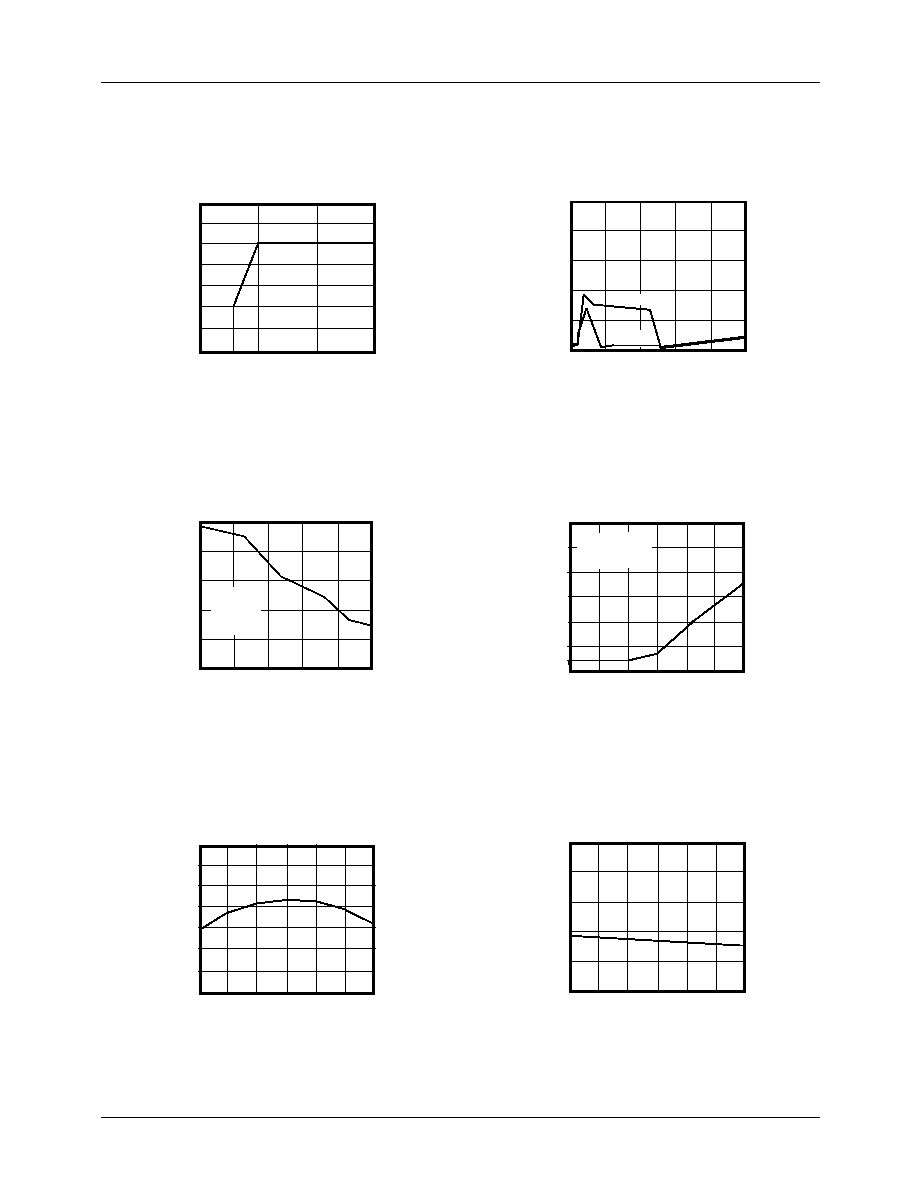
Typical Perfomance Characteristics
Figure 1. Output Voltage vs. Input Voltage
Figure 3. Ripple Rejection vs. Output Voltage
Figure 5. Output Voltage vs. Temperature(Tj)
Figure 2. Quiescent Current vs. Input Voltage
Figure 4. Drop Voltage vs. Output Current
Figure 6. Quiescent Current vs. Temperature(Tj)
FIG.1 Output Voltage
vs. Input Voltage
Input voltage Vin (V)
6
5
4
3
2
1
7
0
0 5 10 15
O
u
t
p
ut
v
o
l
t
age
Vo(
V
)
FIG.3 Ripple Rejection
vs. Output Voltage
Output Current (
)
90
85
75
65
Ri
ppl
e Re
j
e
c
t
i
on Rati
o
(
)
0 20 40 60 80 100
V
IN
= 14V
V
OUT
= 5.0V
f = 120
T
J
= 25
FIG.5 Output Voltage
vs. Temperature(Tj)
Temperature Tj(
)
5.04
5.02
5.00
5.06
-25
O
u
to
u
t
v
o
l
t
a
g
e
V
o
(
V
)
75
125
0
25
50
100
4.96
4.94
4.92
4.98
FIG.2 Quiescent
vs. Input Voltage
Input voltage Vin (V)
10
8.0
6.0
4.0
2.0
0
Q
u
i
e
s
c
ent
c
u
r
r
ent
I
q
(
m
A)
R
L
= 50
0 10 20 30 40 50
R
L
= 500
Output Current (
)
FIG.4 Drop Voltage
vs. Output Current
120
240
200
160
120
0
D
r
opo
ut
v
o
l
t
age
Vdr
op(
)
80
40
80
20
40
60
100
0
VIN
=
14V
V
OUT
= 100
T
J
= 25
FIG.6 Quiescent Current
vs. Temperature(Tj)
Junction temperature Tj(
)
1
0.8
0.6
0.4
0.2
0
Q
u
i
e
sc
e
n
t
cu
r
r
e
n
t
I
q
(
m
A
)
75
125
0
25
50
100
-25
LM2931A
4
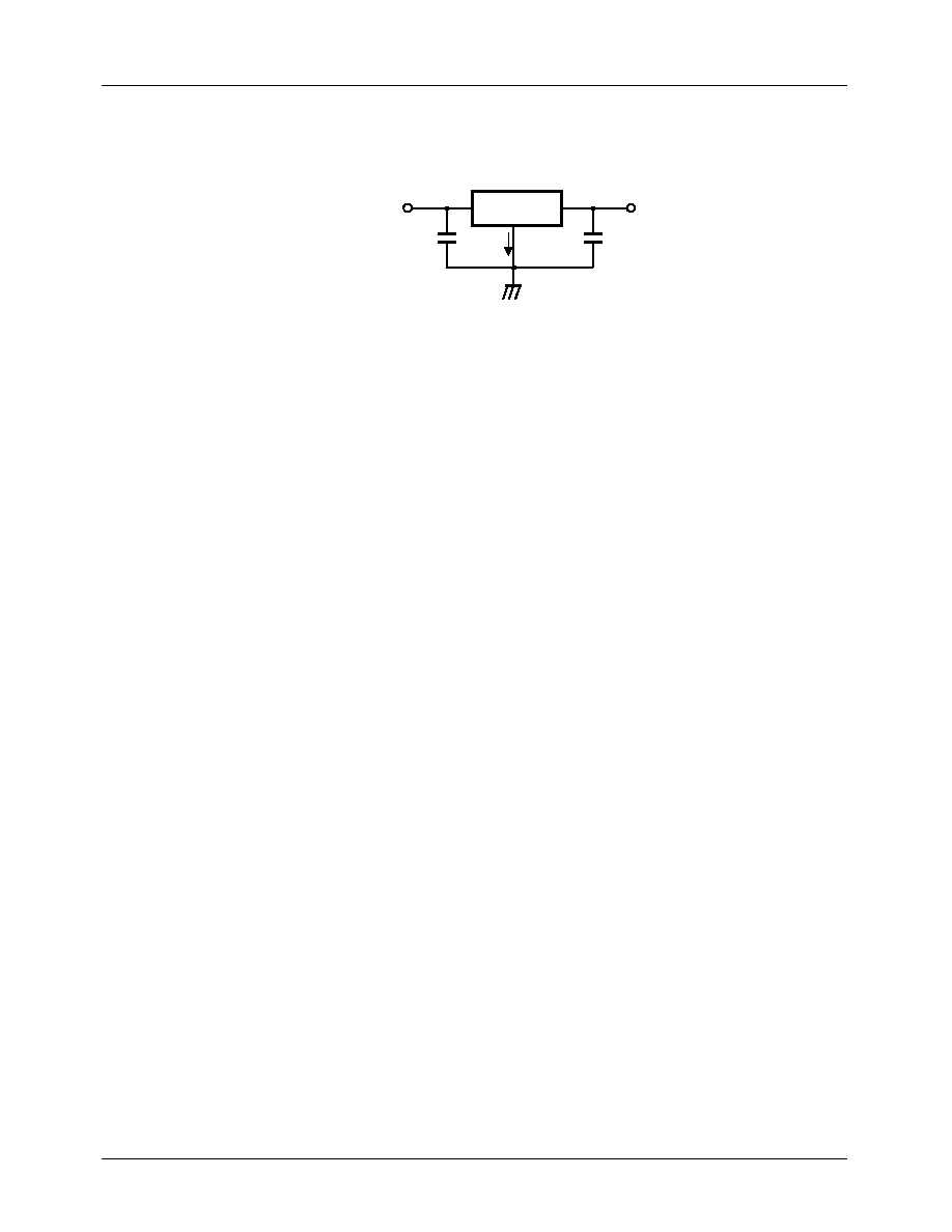
Typical Application
Figure 1. Application Circuit
· Ci is required if regulator is located an appreciable distance from power supply filter.
· Co improves stability .
KA76L05
V
I
V
O
Co
0.1
µ
µ
µ
µ
F
3
1
2
C
I
100
µ
µ
µ
µ
F
I
Q
LM2931A
LM2931A
5
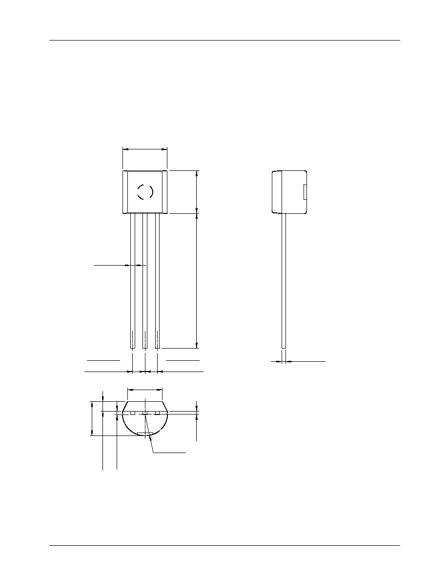
Mechanical Dimensions
Package
Dimensions in millimeters
0.46
±
0.10
1.27TYP
(R2.29)
3.86MAX
[1.27
±
0.20
]
1.27TYP
[1.27
±
0.20
]
3.60
±
0.20
14.47
±
0.40
1.02
±
0.10
(0.25)
4.58
±
0.20
4.58
+0.25
0.15
0.38
+0.10
0.05
0.38
+0.10
0.05
TO-92