 | ÐлекÑÑоннÑй компоненÑ: MCT4 | СкаÑаÑÑ:  PDF PDF  ZIP ZIP |
Äîêóìåíòàöèÿ è îïèñàíèÿ www.docs.chipfind.ru
0.048 (1.22)
0.028 (0.71)
45°
0.046 (1.16)
0.036 (0.92)
4
2
0.195 (4.96)
0.178 (4.52)
0.230 (5.84)
0.209 (5.31)
0.560 (14.22)
0.500 (12.70)
0.210 (5.34)
0.170 (4.32)
3
0.100 (2.54) DIA.
1
0.019 (0.48)
0.016 (0.41)
Ø
4X
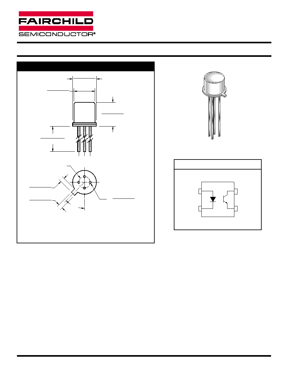
PACKAGE DIMENSIONS
FEATURES
· Hermetically package
· High current transfer ratio; typically 35%
· High isolation resistance; 10
11
ohms at 500 volts
· High voltage isolation emitter to detector
NOTES:
1. Dimensions for all drawings are in inches (mm).
2. Tolerance of ± .010 (.25) on all non-nominal dimensions
unless otherwise specified.
DESCRIPTION
The MCT4 is a standard four-lead, TO-18 package containing a GaAs infrared emitting diode optically coupled to an NPN silicon
planar phototransistor.
2001 Fairchild Semiconductor Corporation
DS300241
8/13/01
1 OF 6
www.fairchildsemi.com
1
3
2
4 EMITTER
COLLECTOR
ANODE
CATHODE
SCHEMATIC
PHOTOTRANSISTOR OPTOCOUPLER
MCT4

www.fairchildsemi.com
2 OF 6
8/13/01
DS300241
Parameter
Symbol
Rating
Unit
Operating Temperature
T
OPR
-55 to +125
°C
Storage Temperature
T
STG
-65 to +150
°C
Soldering Temperature (Flow)
T
SOL-F
260 for 10 sec
°C
EMITTER
P
D
Power Dissipation at 25°C Ambient
(1)
90
mW
Continuous Forward Current
I
F
40 mA
Reverse Voltage
V
R
3
V
Forward Current - Peak (1 µs pulse, 300 pps)
I
F
(pk)
3.0
A
DETECTOR
P
D
Power Dissipation 25°C Ambient
(2)
200
mW
Collector to Emitter Voltage
V
CEO
30
V
Emitter to Collector Voltage
V
ECO
7
V
COUPLER
Total Power Dissipation
(3)
P
D
250
mW
Isolation Voltage
1000
VDC
ABSOLUTE MAXIMUM RATINGS
(T
A
= 25°C unless otherwise specified)
ELECTRICAL / OPTICAL CHARACTERISTICS
(T
A
=25°C)
PHOTOTRANSISTOR OPTOCOUPLER
MCT4
Parameters
Test Conditions
Symbol
Min
Typ
Max
Units
EMITTER
Forward Voltage
I
F
= 40 mA
V
F
1.30
1.50
V
Reverse Current
V
R
= 3.0 V
I
R
0.15
10
µA
Capacitance
V = 0 V
C
150
pF
DETECTOR
Breakdown Voltage
Collector to Emitter
I
C
= 1.0 mA, I
F
= 0
BV
CEO
30
V
Emitter to Collector
I
E
= 100
µ
A, I
F
= 0
BV
ECO
7
12
V
Leakage Current
Collector to Emitter
V
CE
= 10 V, I
F
= 0
I
CEO
5
50
nA
Capacitance
pF
Collector to Emitter
V
CE
= 0
C
CE
2
INDIVIDUAL COMPONENT CHARACTERISTICS
NOTE:
1. Derate power linearly 1.2 mW/°C above 25°C
2. Derate power linearly 2.67 mW/°C above 25°C
3. Derate power linearly 3.3 mW/°C above 25°C

DC Characteristics
Test Conditions
Symbol
Min
Typ
Max
Units
COUPLED
CTR
DC current Transfer Ratio (note 1)
V
CE
= 10 V, I
F
= 10 mA
15
35
%
Saturation Voltage
I
C
= 500
µ
A, I
F
= 10 mA
V
CE(SAT)
0.1
V
I
C
= 2 mA, I
F
= 50 mA
0.2
0.5
AC Characteristics
Test Conditions
Symbol
Min
Typ
Max
Units
Capacitance LED to Detector
1.8
pF
Bandwidth (Fig. 5)
Note 2
300
kHz
Rise Time and Fall Time (see operating schematic)
I
C
= 2 mA, V
CE
= 10 V, Note 3
2
µ
s
TRANSFER CHARACTERISTICS
(T
A
= 25°C Unless otherwise specified.)
PHOTOTRANSISTOR OPTOCOUPLER
MCT4
DS300241
8/13/01
3 OF 6
www.fairchildsemi.com
NOTE:
1. The current transfer ratio (I
C
/I
F
) is the ratio of the detector collector current to the LED input current with V
CE
at 10 volts.
2. The frequency at which i
c
is 3 dB down from the 1 kHz value.
3. Rise time (t
r
) is the time required for the collector current to increase from 10% of its final value, to 90%. Fall time (t
f
) is the time required
for the collector current to decrease from 90% of its initial value to 10%.
Characteristic
Test Conditions
Symbol
Min
Typ
Max
Units
Isolation Resistance
V = 500 VDC
R
ISO
10
11
10
12
!
Breakdown Voltage
Time = 1 sec
1000
1500
VDC
ISOLATION CHARACTERISTICS
www.fairchildsemi.com
4 OF 6
813/01
DS300241
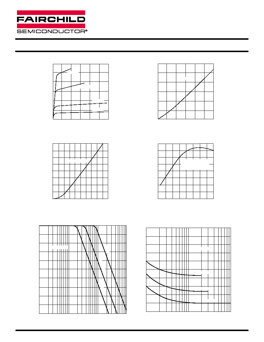
Figure 1. Detector Output Characteristics
I
C
, COLLECTOR CURRENT DETECTOR (mA)
5
10
15
20
25
20
5
V
CE
, COLLECTOR VOLTAGE DETECTOR (V)
10
15
20
25
30
I
F
= 60 mA
I
F
= 40 mA
I
F
= 20 mA
I
F
= 10 mA
Figure 2. Input Current vs. Output Current
I
C
, COLLECTOR CURRENT DETECTOR (mA)
5
0
10
15
20
25
20
10
0
I
F
, INPUT CURRENT LED (mA)
20
30
40
50
60
V
CE
= 10 VOLTS
Figure 3. Dark Current vs. Temperature
I
CEO,
DARK CURRENT (A)
10
-4
10
-5
10
-6
10
-7
10
-8
10
-9
10
-10
10
-11
10
-12
-40
-60
T
A
, AMBIENT TEMPERATURE (
°
C)
-20
0
20
40
60
80
100 120 140
V
CE
= 10 VOLTS
Figure 4. Current Output vs. Temperature
CTR
,
NORMALIZED (%)
110
100
90
80
70
60
50
40
30
-40
-60
T
A
, AMBIENT TEMPERATURE (
°
C)
-20
0
20
40
60
80
100
0.2
0.1
I
C
, COLLECTOR CURRENT (mA)
0.3
0.4
0.6 0.8 1
2
3
4
5 6 7 8 10
LED CURRENT - 10 mA
V
CE
= 10 VOLTS
FREE STANDING DEVICE
Figure 5. Output vs. Frequency
Figure 6. Switching Time vs. Collector Current
COLLECTOR CURRENT (mA)
2.0
1.8
1.6
1.4
1.2
1.0
0.8
0.6
0.4
0.2
SWITCHING TIME (
µ
s)
12
10
8
6
4
2
1K
1
10K
100K
FREQUENCY (Hz)
V
CE
= 10 VOLTS
R
L
= 100
R
L
= 470
R
L
= 1000
V
CE
= 10 VOLTS
R
L
= 1000
R
L
= 470
R
L
= 100
PHOTOTRANSISTOR OPTOCOUPLER
MCT4
PHOTOTRANSISTOR OPTOCOUPLER
MCT4
DS300241
8/13/01
5 OF 6
www.fairchildsemi.com
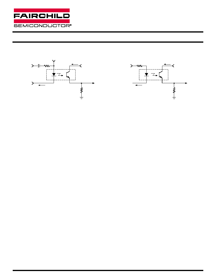
Figure 7. Modulation Circuit Used to Obtain Output vs.
Frequency Plot
LED
MODULATION
INPUT
DETECTOR
OUTPUT
V
CC
= 10 VOLTS
R
L
= 100
CONSTANT
CURRENT
INPUT
47
1
µ
F
I
F
I
C
Figure 8. Circuit Used to Obtain Switching Time vs.
Collector Current Plot
LED
PULSE
INPUT
DETECTOR
PULSE
OUTPUT
V
CC
= 10 VOLTS
R
L
= 100
47
I
F
I
C