 | ÐлекÑÑоннÑй компоненÑ: MCT5200 | СкаÑаÑÑ:  PDF PDF  ZIP ZIP |
Äîêóìåíòàöèÿ è îïèñàíèÿ www.docs.chipfind.ru
6/10/03
Page 1 of 11
© 2003 Fairchild Semiconductor Corporation
MCT5200
MCT5201
MCT5210
MCT5211
LOW INPUT CURRENT
PHOTOTRANSISTOR OPTOCOUPLERS
Description
The MCT52XX series consists of a high-efficiency AlGaAs, infrared emitting
diode, coupled with an NPN phototransistor in a six pin dual-in-line package.
The MCT52XX is well suited for CMOS to LSTT/TTL interfaces, offering
250% CTR
CE(SAT)
with 1 mA of LED input current. When an LED input
current of 1.6 mA is supplied data rates to 20K bits/s are possible.
The MCT52XX can easily interface LSTTL to LSTTL/TTL, and with use of an
external base to emitter resistor data rates of 100K bits/s can be achieved.
Features
·
High CTR
CE(SAT)
comparable to Darlingtons
·
CTR guaranteed 0°C to 70°C
·
High common mode transient rejection 5kV/µs
·
Data rates up to 150 kbits/s (NRZ)
·
Underwriters Laboratory (UL) recognized (file #E90700)
·
VDE recognized (file #94766)
Add option 300 (e.g., MCT5211.300)
Applications
·
CMOS to CMOS/LSTTL logic isolation
·
LSTTL to CMOS/LSTTL logic isolation
·
RS-232 line receiver
·
Telephone ring detector
·
AC line voltage sensing
·
Switching power supply
Parameters
Symbol
Device
Value
Units
TOTAL DEVICE
Storage Temperature
T
STG
All
-55 to +150
°C
Operating Temperature
T
OPR
All
-55 to +100
°C
Lead Solder Temperature
T
SOL
All
260 for 10 sec
°C
Total Device Power Dissipation @ 25°C (LED plus detector)
P
D
All
260
mW
Derate Linearly From 25°C
3.5
mW/°C
EMITTER
Continuous Forward Current
I
F
All
50
mA
Reverse Input Voltage
V
R
All
6
V
Forward Current - Peak (1 µs pulse, 300 pps)
I
F
(pk)
All
3.0
A
LED Power Dissipation
P
D
All
75
mW
Derate Linearly From 25°C
All
1.0
mW/°C
DETECTOR
Continuous Collector Current
I
C
All
150
mA
Detector Power Dissipation
P
D
All
150
mW
Derate Linearly from 25°C
All
2.0
mW/°C
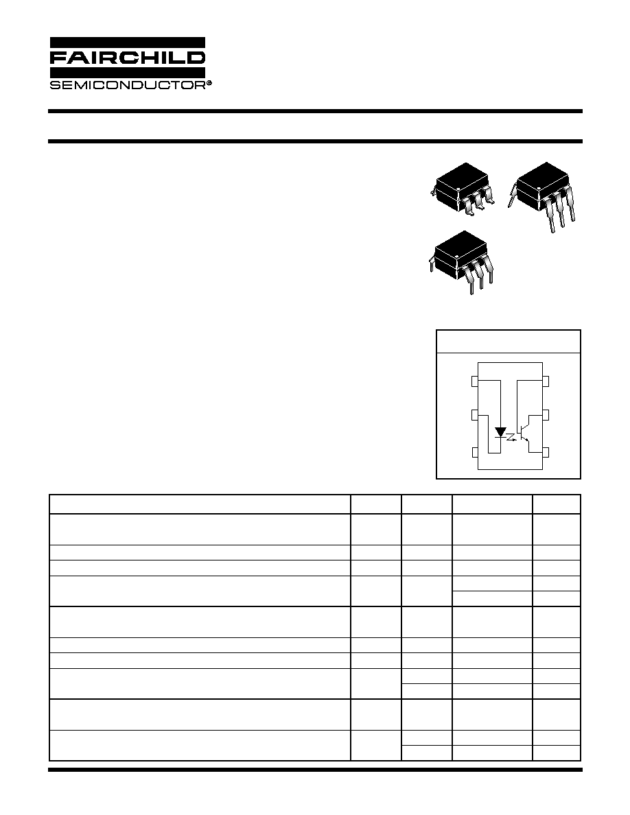
SCHEMATIC
6
1
6
1
6
1
1
2
6
5 COL
4 EMITTER
BASE
ANODE
CATHODE
3
6/10/03
LOW INPUT CURRENT
PHOTOTRANSISTOR OPTOCOUPLERS
Page 2 of 11
© 2003 Fairchild Semiconductor Corporation
MCT5200
MCT5201
MCT5210
MCT5211
**All typical T
A
=25°C
ELECTRICAL CHARACTERISTICS
(T
A
= 25°C Unless otherwise specified.)
INDIVIDUAL COMPONENT CHARACTERISTICS
Parameters
Test Conditions
Symbol
Device
Min
Typ**
Max
Units
EMITTER
Input Forward Voltage
(I
F
= 5 mA)
V
F
All
1.25
1.5
V
Forward Voltage Temp.
Coefficient
(I
F
= 2 mA)
V
F
T
A
All
-1.75
mV/
°C
Reverse Voltage
(I
R
= 10 µA)
V
R
All
6
V
Junction Capacitance
(V
F
= 0 V, f = 1.0 MHz)
C
J
All
18
pF
DETECTOR
Collector-Emitter Breakdown Voltage
(I
C
= 1.0 mA, I
F
= 0)
BV
CEO
All
30
100
V
Collector-Base Breakdown Voltage
(I
C
= 10 µA, I
F
= 0)
BV
CBO
All
30
120
V
Emitter-Base Breakdown Voltage
(I
C
= 10 µA, I
F
= 0)
BV
EBO
All
5
10
V
Collector-Emitter Dark Current
(V
CE
= 10V, I
F
= 0, R
BE
= 1M
)
I
CER
All
1
100
nA
Capacitance
Collector to Emitter
(V
CE
= 0, f = 1 MHz)
C
CE
All
10
pF
Collector to Base
(V
CB
= 0, f = 1 MHz)
C
CB
All
80
pF
Emitter to Base
(V
EB
= 0, f = 1 MHz)
C
EB
All
15
pF
ISOLATION CHARACTERISTICS
Characteristic
Test Conditions
Symbol
Device
Min
Typ**
Max
Units
Input-Output Isolation
Voltage
(10)
(f = 60Hz, t = 1 min.)
V
ISO
All
5300
Vac(rms)
Isolation Resistance
(10)
V
I-O
= 500 VDC, T
A
= 25°C
R
ISO
All
10
11
Isolation Capacitance
(9)
V
I-O
= 0, f = 1 MHz
C
ISO
All
0.7
pF
Common Mode Transient
V
CM
= 50 V
P-P1
, R
L
= 750
, I
F
= 0
CM
H
MCT5210/11
5000
V/µs
Rejection Output High
V
CM
= 50 V
P-P
, R
L
= 1K
, I
F
= 0
MCT5200/01
Common Mode Transient
V
CM
= 50 V
P-P1
, R
L
= 750
, I
F
=1.6mA
CM
L
MCT5210/11
5000
V/µs
Rejection Output Low
V
CM
= 50 V
P-P1
, R
L
= 1K
, I
F
= 5 mA
MCT5200/01
6/10/03
Page 3 of 11
© 2003 Fairchild Semiconductor Corporation
LOW INPUT CURRENT
PHOTOTRANSISTOR OPTOCOUPLERS
MCT5200
MCT5201
MCT5210
MCT5211
TRANSFER CHARACTERISTICS
(T
A
= 0°C to 70°C Unless otherwise specified.)
DC Characteristics
Test Conditions
Symbol
Device
Min
Typ**
Max
Units
Saturated Current
Transfer Ratio
(1)
(Collector to Emitter)
I
F
= 10 mA, V
CE
= 0.4 V
CTR
CE(SAT)
MCT5200
75
%
I
F
= 5 mA, V
CE
= 0.4 V
MCT5201
120
I
F
= 3.0 mA, V
CE
= 0.4 V
MCT5210
60
I
F
= 1.6 mA, V
CE
= 0.4 V
MCT5211
100
I
F
= 1.0 mA, V
CE
= 0.4 V
75
Current Transfer Ratio
(Collector to Emitter)
(1)
I
F
= 3.0 mA, V
CE
= 5.0 V
CTR
(CE)
MCT5210
70
%
I
F
= 1.6 mA, V
CE
= 5.0 V
MCT5211
150
I
F
= 1.0 mA, V
CE
= 5.0 V
110
Current Transfer Ratio
Collector to Base(2)
I
F
= 10 mA, V
CB
= 4.3 V
CTR
(CB)
MCT5200
0.2
%
I
F
= 5 mA, V
CB
= 4.3 V
MCT5201
0.28
I
F
= 3.0 mA, V
CE
= 4.3 V
MCT5210
0.2
I
F
= 1.6 mA, V
CE
= 4.3 V
MCT5211
0.3
I
F
= 1.0 mA, V
CE
= 4.3 V
0.25
Saturation Voltage
I
F
= 10 mA, I
CE
= 7.5 mA
V
CE(SAT)
MCT5200
0.4
V
I
F
= 5 mA, I
CE
= 6 mA
MCT5201
0.4
I
F
= 3.0 mA, I
CE
= 1.8 mA
MCT5210
0.4
I
F
= 1.6 mA, I
CE
= 1.6 mA
MCT5211
0.4
AC Characteristics
Test Conditions
Symbol
Device
Min
Typ
Max
Units
Propagation Delay
High to Low
(3)
R
L
= 330
, R
BE
=
I
F
= 3.0 mA
T
PHL
MCT5210
10
µs
R
L
= 3.3 k
, R
BE
= 39 k
V
CC
= 5.0 V
7
R
L
= 750
, R
BE
=
I
F
= 1.6mA
MCT5211
14
R
L
= 4.7 k
, R
BE
= 91 k
V
CC
= 5.0V
15
R
L
= 1.5 k
, R
BE
=
I
F
= 1.0mA
17
R
L
= 10 k
, R
BE
= 160 k
V
CC
= 5.0V
24
V
CE
= 0.4V, V
CC
= 5V,
R
L
= fig. 13, R
BE
= 330 k
I
F
= 10mA
MCT5200
1.6
12
I
F
= 5mA
MCT5201
3
30
Propagation Delay
Low to High
(4)
R
L
= 330
, R
BE
=
I
F
= 3.0 mA
T
PLH
MCT5210
0.4
µs
R
L
= 3.3 k
, R
BE
= 39 k
V
CC
= 5.0 V
8
R
L
= 750
, R
BE
=
I
F
= 1.6mA
MCT5211
2.5
R
L
= 4.7 k
, R
BE
= 91 k
V
CC
= 5.0V
11
R
L
= 1.5 k
, R
BE
=
I
F
= 1.0mA
7
R
L
= 10 k
, R
BE
= 160 k
V
CC
= 5.0 V
16
V
CE
= 0.4V, V
CC
= 5V,
R
L
= fig. 13, R
BE
= 330 k
I
F
= 10mA
MCT5200
18
20
I
F
= 5mA
MCT5201
12
13
Delay Time
(5)
V
CE
= 0.4V,
R
BE
= 330 k
,
R
L
= 1 k
, V
CC
= 5V
I
F
= 10mA
t
d
MCT5200
0.5
7
µs
I
F
= 5mA
MCT5201
1.1
15
Rise Time
(6)
V
CE
= 0.4V,
R
BE
= 330 k
,
R
L
= 1 k
, V
CC
= 5V
I
F
= 10mA
t
r
MCT5200
1.3
6
µs
I
F
= 5mA
MCT5201
2.5
20

6/10/03
LOW INPUT CURRENT
PHOTOTRANSISTOR OPTOCOUPLERS
Page 4 of 11
© 2003 Fairchild Semiconductor Corporation
MCT5200
MCT5201
MCT5210
MCT5211
**All typicals at T
A
= 25°C
Notes
1. DC Current Transfer Ratio (CTR
CE
) is defined as the transistor collector current (I
CE
) divided by the input LED current (I
F
) x
100%, at a specified voltage between the collector and emitter (V
CE
).
2. The collector base Current Transfer Ratio (CTR
CB
) is defined as the transistor collector base photocurrent(I
CB
) divided by the
input LED current (I
F
) time 100%.
3. Referring to Figure 14 the T
PHL
propagation delay is measured from the 50% point of the rising edge of the data input pulse to
the 1.3V point on the falling edge of the output pulse.
4. Referring to Figure 14 the T
PLH
propagation delay is measured from the 50% point of the falling edge of data input pulse to the
1.3V point on the rising edge of the output pulse.
5. Delay time (t
d
) is measured from 50% of rising edge of LED current to 90% of Vo falling edge.
6. Rise time (t
r
) is measured from 90% to 10% of Vo falling edge.
7. Storage time (t
s
) is measured from 50% of falling edge of LED current to 10% of Vo rising edge.
8. Fall time (t
f
) is measured from 10% to 90% of Vo rising edge.
9. C
ISO
is the capacitance between the input (pins 1, 2, 3 connected) and the output, (pin 4, 5, 6 connected).
10. Device considered a two terminal device: Pins 1, 2, and 3 shorted together, and pins 5, 6 and 7 are shorted together.
Storage Time
(7)
V
CE
= 0.4V,
R
BE
= 330 k
,
R
L
= 1 k
, V
CC
= 5V
I
F
= 10mA
t
s
MCT5200
15
18
µs
I
F
= 5mA
MCT5201
10
13
Fall Time
(8)
V
CE
= 0.4V,
R
BE
= 330 k
,
R
L
= 1 k
, V
CC
= 5V
I
F
= 10mA
t
f
MCT5200
16
30
µs
I
F
= 5mA
MCT5201
16
30
TRANSFER CHARACTERISTICS
(T
A
= 0°C to 70°C Unless otherwise specified.) (Continued)
DC Characteristics
Test Conditions
Symbol
Device
Min
Typ**
Max
Units

6/10/03
Page 5 of 11
© 2003 Fairchild Semiconductor Corporation
LOW INPUT CURRENT
PHOTOTRANSISTOR OPTOCOUPLERS
MCT5200
MCT5201
MCT5210
MCT5211
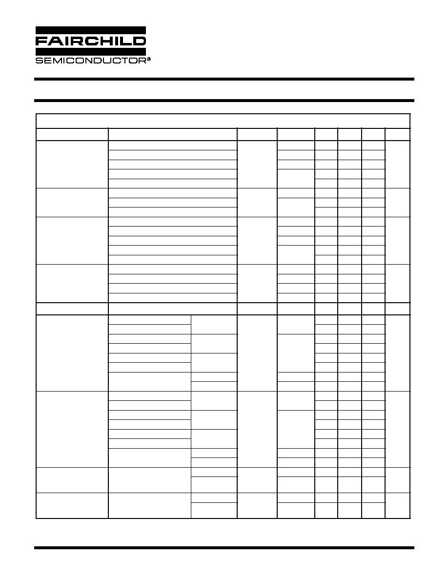
TYPICAL PERFORMANCE GRAPHS
Fig. 1 LED Forward Voltage vs. Forward Current
Fig. 2 Normalized Current Transfer Ratio vs.
Forward Current
Fig. 3 Normalized CTR vs. Temperature
Fig. 4 Normalized Collector vs.
Collector - Emitter Voltage
Fig. 5 Normalized Collector Base Photocurrent
Ratio vs. Forward Current
Fig. 6 Normalized Collector -
Base Current vs. Temperature
2.0
1.8
1.6
1.4
1.2
1.0
0.8
0.1
1
10
V
F
- FORWARD VOLTAGE (V)
1.6
10
1
0.1
0.01
0.001
0.0001
1.2
1.4
1.0
0.8
0.6
0.4
0.2
0.0
100
10
1
0.1
0.01
10
1
0.1
0.01
0.001
NORMALIZED CTR
CE
NORMALIZED ICB - COLLECTOR
BASE PHOTO CURRENT
NORMALIZED - COLLECTOR
BASE CURRENT
NORMALIZED I
CE
- COLLECTOR
- EMITTER CURRENT
1.2
1.0
0.8
0.6
0.4
0.2
0
NORMALIZED CTR
CE
I
F
- LED FORWARD CURRENT (mA)
T
A
- AMBIENT TEMPERATURE - °C
T
A
- AMBIENT TEMPERATURE - °C
I
F
- FORWARD CURRENT - mA
V
CE
- COLLECTOR - EMITTER VOLTAGE - V
I
F
- FORWARD CURRENT (mA)
100
0.1
-60
-40
-20
0
20
40
60
80
100
-60
-40
-20
0
20
40
60
80
100
0.1
1
10
0.1
1
100
10
1
10
100
T
A
= -55°C
T
A
= 25°C
T
A
= 100°C
Normalized to:
I
F
= 5mA
V
CE
= 5V
T
A
= 25°C
Normalized to:
I
F
= 5mA
V
CE
= 5V
T
A
= 25°C
I
F
= 1mA
I
F
= 10mA
I
F
= 2mA
I
F
= 5mA
I
F
= 0.5 mA
I
F
= 0.2 mA
:
Normalized to:
I
F
= 5mA
V
CE
= 5V
T
A
= 25°C
I
F
= 0.2 mA
I
F
= 0.5 mA
I
F
= 1 mA
I
F
= 2 mA
I
F
= 5 mA
I
F
= 10 mA
Normalized to:
I
F
= 5mA
V
CB
= 4.3V
T
A
= 25°C
Normalized to:
I
F
= 5mA
V
CB
= 4.3V
T
A
= 25°C
I
F
= 0.2 mA
I
F
= 0.5 mA
I
F
= 1 mA
I
F
= 2 mA
I
F
= 5 mA
I
F
= 10 mA