© 2000 Fairchild Semiconductor Corporation
DS005217
www.fairchildsemi.com
February 1984
Revised August 2000
MM74HC4538 Dual Retr
igg
e
rabl
e
Monost
a
bl
e
Mul
t
i
v
ibr
a
tor
MM74HC4538
Dual Retriggerable Monostable Multivibrator
General Description
The MM74HC4538 high speed monostable multivibrator
(one shots) is implemented in advanced silicon-gate
CMOS technology. They feature speeds comparable to low
power Schottky TTL circuitry while retaining the low power
and high noise immunity characteristic of CMOS circuits.
Each multivibrator features both a negative, A, and a posi-
tive, B, transition triggered input, either of which can be
used as an inhibit input. Also included is a clear input that
when taken low resets the one shot. The MM74HC4538 is
retriggerable. That is, it may be triggered repeatedly while
their outputs are generating a pulse and the pulse will be
extended.
Pulse width stability over a wide range of temperature and
supply is achieved using linear CMOS techniques. The out-
put pulse equation is simply: PW
=
0.7(R)(C) where PW is
in seconds, R is in ohms, and C is in farads. This device is
pin compatible with the CD4528, and the CD4538 one
shots. All inputs are protected from damage due to static
discharge by diodes to V
CC
and ground.
Features
s
Schmitt trigger on A and B inputs
s
Wide power supply range: 2≠6V
s
Typical trigger propagation delay: 32 ns
s
Fanout of 10 LS-TTL loads
s
Low input current: 1
µ
A max
Ordering Code:
Devices also available in Tape and Reel. Specify by appending the suffix letter "X" to the ordering code.
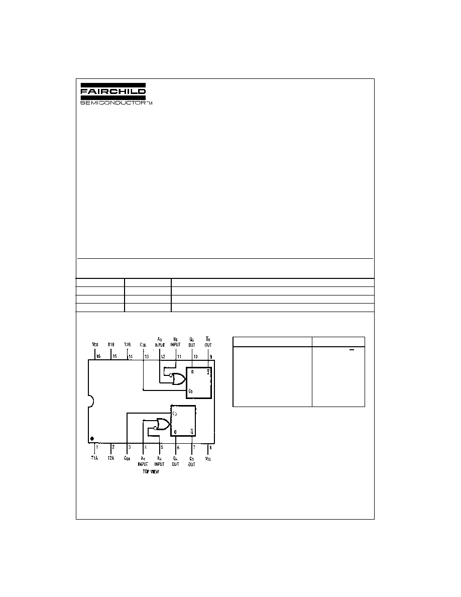
Connection Diagram
Truth Table
H
=
HIGH Level
L
=
LOW Level
=
Transition from LOW-to-HIGH
=
Transition from HIGH-to-LOW
�
=
One HIGH Level Pulse
=
One LOW Level Pulse
X
=
Irrelevant
Order Number
Package Number
Package Description
MM74HC4538M
M16A
16-Lead Small Outline Integrated Circuit (SOIC), JEDEC MS-012, 0.150 Narrow
MM74HC4538SJ
M16D
16-Lead Small Outline Package (SOP), EIAJ TYPE II, 5.3mm Wide
MM74HC4538N
N16E
16-Lead Plastic Dual-In-Line Package (PDIP), JEDEC MS-001, 0.300 Wide
Inputs Outputs
Clear
A
B
Q
Q
L
X
X
L
H
X
H
X
L
H
X
X
L
L
H
H
L
�
H
H
�
www.fairchildsemi.com
2
M
M
74HC4538
Block Diagrams
Note: Pin 1 and Pin 15 must be hard-wired to GND.
Logic Diagram
3
www.fairchildsemi.com
MM74HC4538
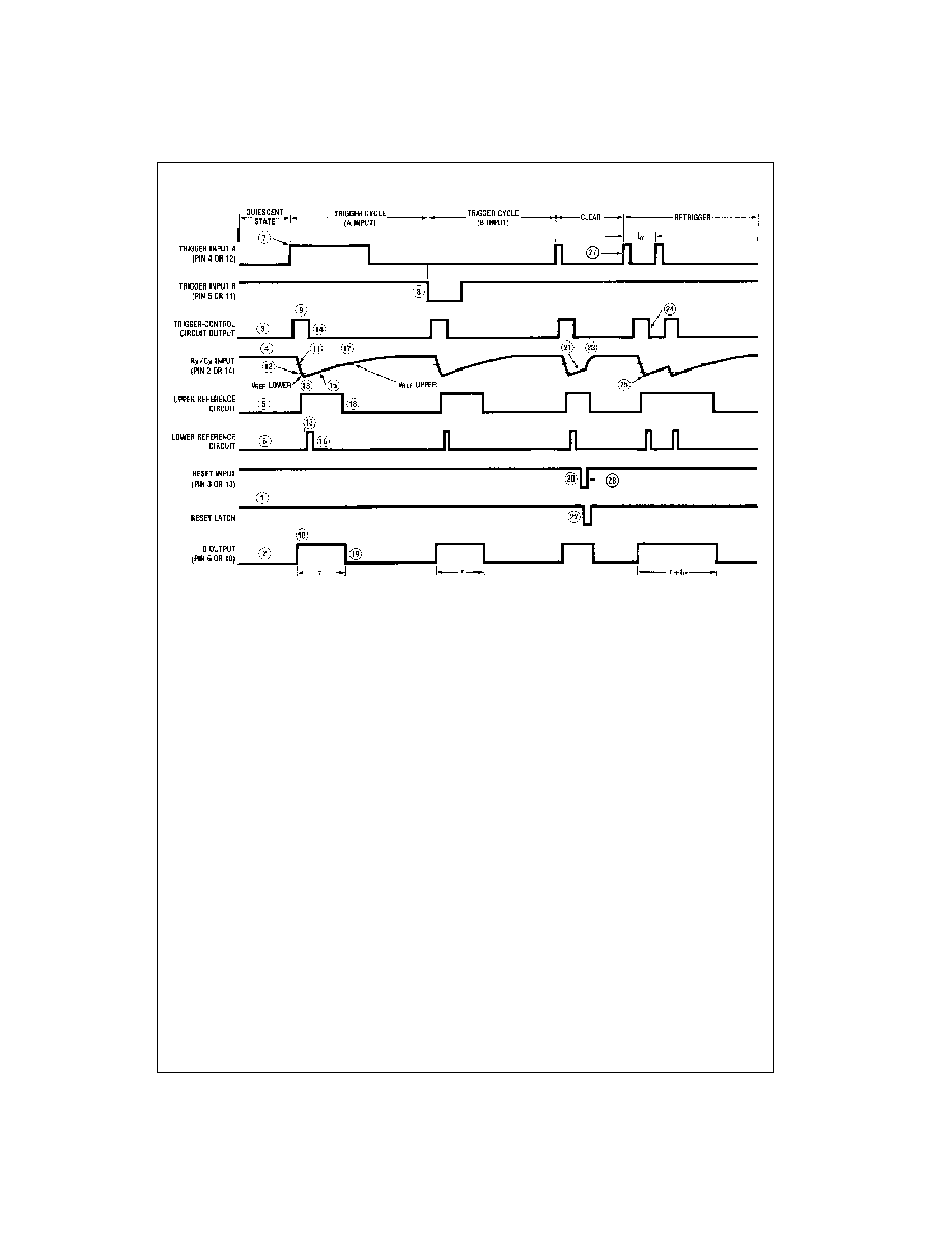
Timing Diagram
Circuit Operation
The MM74HC4538 operates as follows (refer to logic dia-
gram). In the quiescent state, the external timing capacitor,
C
X
, is charged to V
CC
. When a trigger occurs, the Q output
goes HIGH and C
X
discharges quickly to the lower refer-
ence voltage (V
REF
Lower
=
1
/
3
V
CC
). C
X
then charges,
through R
X
, back up to the upper reference voltage (V
REF
Upper
=
2
/
3
V
CC
), at which point the one-shot has timed out
and the Q output goes LOW.
The following, more detailed description of the circuit oper-
ation refers to both the logic diagram and the timing dia-
gram.
QUIESCENT STATE
In the quiescent state, before an input trigger appears, the
output latch is HIGH and the reset latch is HIGH (#1 in logic
diagram).
Thus the Q output (pin 6 or 10) of the monostable multivi-
brator is LOW (#2, timing diagram).
The output of the trigger-control circuit is LOW (#3), and
transistors M1, M2, and M3 are turned off. The external
timing capacitor, C
X
, is charged to V
CC
(#4), and the upper
reference circuit has a LOW output (#5). Transistor M4 is
turned ON and transmission gate T1 is turned OFF. Thus
the lower reference circuit has V
CC
at the noninverting
input and a resulting LOW output (#6).
In addition, the output of the trigger-control reset circuit is
LOW.
TRIGGER OPERATION
The MM74HC4538 is triggered by either a rising-edge sig-
nal at input A (#7) or a falling-edge signal at input B (#8),
with the unused trigger input and the Reset input held at
the voltage levels shown in the Truth Table. Either trigger
signal will cause the output of the trigger-control circuit to
go HIGH (#9).
The trigger-control circuit going HIGH simultaneously ini-
tiates three events. First, the output latch goes LOW, thus
taking the Q output of the HC4538 to a HIGH State (#10).
Second, transistor M3 is turned on, which allows the exter-
nal timing capacitor, C
X
, to rapidly discharge toward
ground (#11). (Note that the voltage across C
X
appears at
the input of the upper reference circuit comparator.) Third,
transistor M4 is turned off and transmission gate T1 is
turned ON, thus allowing the voltage across C
X
to also
appear at the input of the lower reference circuit compara-
tor.
When C
X
discharges to the reference voltage of the lower
reference circuit (#12), the outputs of both reference cir-
cuits will be HIGH (#13). The trigger-control reset circuit
goes HIGH, resetting the trigger-control circuit flip-flop to a
LOW State (#14). This turns transistor M3 OFF again,
allowing C
X
to begin to charge back up toward V
CC
, with a
time constant t
=
R
X
C
X
(#15). In addition, transistor M4 is
turned ON and transmission gate T1 is turned OFF. Thus a
high voltage level is applied to the input of the lower refer-
ence circuit comparator, causing its output to go LOW
(#16). The monostable multivibrator may be retriggered at
any time after the trigger-control circuit goes LOW.
When C
X
charges up to the reference voltage of the upper
reference circuit (#17), the output of the upper reference
circuit goes LOW (#18). This causes the output latch to

www.fairchildsemi.com
4
M
M
74HC4538
Circuit Operation
(Continued)
toggle, taking the Q output of the HC4538 to a LOW State
(#19), and completing the time-out cycle.
RESET OPERATION
A low voltage applied to the Reset pin always forces the Q
output of the HC4538 to a LOW State.
The timing diagram illustrates the case in which reset
occurs (#20) while C
X
is charging up toward the reference
voltage of the upper reference circuit (#21). When a reset
occurs, the output of the reset latch goes LOW (#22), turn-
ing ON transistor M1. Thus C
X
is allowed to quickly charge
up to V
CC
(#23) to await the next trigger signal.
Recovery time is the required delay after reset goes inac-
tive to a new trigger rising edge. On the diagram it is shown
as (#26) to (#27).
RETRIGGER OPERATION
In the retriggerable mode, the HC4538 may be retriggered
during timing out of the output pulse at any time after the
trigger-control circuit flip-flop has been reset (#24).
Because the trigger-control circuit flip-flop resets shortly
after C
X
has discharged to the reference voltage of the
lower reference circuit (#25), the minimum retrigger time, t
rr
is a function of internal propagation delays and the dis-
charge time of C
X
:
at room temperature
POWER-DOWN CONSIDERATIONS
Large values of C
X
may cause problems when powering
down the MM74HC4538 because of the amount of energy
stored in the capacitor. When a system containing this
device is powered down, the capacitor may discharge from
V
CC
through the input protection diodes at pin 2 or pin 14.
Current through the protection diodes must be limited to 30
mA; therefore, the turn-off time of the V
CC
power supply
must not be faster than t
=
V
CC
∑C
X
/(30 mA). For example, if
V
CC
=
5V and C
X
=
15
µ
F, the V
CC
supply must turn OFF
no faster than t
=
(15V)∑(15
µ
F)/30 mA
=
2.5 ms. This is
usually not a problem because power supplies are heavily
filtered and cannot discharge at this rate.
When a more rapid decrease of V
CC
to zero volts occurs,
the MM74HC4538 may sustain damage. To avoid this pos-
sibility, use an external clamping diode, D
X
, connected
from V
CC
to the C
X
pin.
SET UP RECOMMENDATIONS
Minimum
R
X
=
1 k
Minimum
C
X
=
0 pF.
5
www.fairchildsemi.com
MM74HC4538
Absolute Maximum Ratings
(Note 1)
(Note 2)
Recommended Operating
Conditions
Note 1: Maximum Ratings are those values beyond which damage to the
device may occur.
Note 2: Unless otherwise specified all voltages are referenced to ground.
Note 3: Power Dissipation Temperature Derating: Plastic "N" Package:
-
12mW/
∞
C from 65
∞
C to 85
∞
C.
DC Electrical Characteristics
(Note 4)
Note 4: For a power supply of 5V
±
10% the worst case output voltages (V
OH
, and V
OL
) occur for HC at 4.5V. Thus the 4.5V values should be used when
designing with this supply. Worst case V
IH
and V
IL
occur at V
CC
=
5.5V and 4.5V respectively. (The V
IH
value at 5.5V is 3.85V.) The worst case leakage cur-
rent (I
IN
, I
CC
, and I
OZ
) occur for CMOS at the higher voltage and so the 6.0V values should be used.
Supply Voltage (V
CC
)
-
0.5 to
+
7.0V
DC Input Voltage (V
IN
)
-
1.5 to V
CC
+
1.5V
DC Output Voltage (V
OUT
)
-
0.5 to V
CC
+
0.5V
Clamp Diode Current (I
IK
, I
OK
)
±
20 mA
DC Output Current, per pin (I
OUT
)
±
25 mA
DC V
CC
or GND Current, per pin (I
CC
)
±
50 mA
Storage Temperature Range (T
STG
)
-
65
∞
C to
+
150
∞
C
Power Dissipation (P
D
)
(Note 3)
600 mW
S.O. Package only
500 mW
Lead Temperature (T
L
)
(Soldering 10 seconds)
260
∞
C
Min
Max
Units
Supply Voltage (V
CC
)
2
6
V
DC Input or Output Voltage
0
V
CC
V
(V
IN
, V
OUT
)
Operating Temperature Range (T
A
)
-
40
+
85
∞
C
Input Rise or Fall Times
(Reset only)
(t
r
, t
f
) V
CC
=
2.0V
1000
ns
V
CC
=
4.5V
500
ns
V
CC
=
6.0V
400
ns
Symbol
Parameter
Conditions
V
CC
T
A
=
25
∞
C
T
A
=
-
40 to 85
∞
C T
A
=
-
55 to 125
∞
C
Units
Typ
Guaranteed Limits
V
IH
Minimum HIGH Level Input
2.0V
1.5
1.5
1.5
V
Voltage
4.5V
3.15
3.15
3.15
V
6.0V
4.2
4.2
4.2
V
V
IL
Maximum LOW Level Input
2.0V
0.5
0.5
0.5
V
Voltage 4.5V
1.35
1.35
1.35
V
6.0V
1.8
1.8
1.8
V
V
OH
Minimum HIGH Level Output V
IN
=
V
IH
or V
IL
Voltage
|I
OUT
|
20
µ
A
2.0V
2.0
1.9
1.9
1.9
V
4.5V
4.5
4.4
4.4
4.4
V
6.0V
6.0
5.9
5.9
5.9
V
V
IN
=
V
IH
or V
IL
|I
OUT
|
4.0 mA
4.5V
3.98
3.84
3.7
V
|I
OUT
|
5.2 mA
6.0V
5.48
5.34
5.2
V
V
OL
Maximum LOW Level Output V
IN
=
V
IH
or V
IL
2.0V
0
0.1
0.1
0.1
V
Voltage
|I
OUT
|
20
µ
A
4.5V
0
0.1
0.1
0.1
V
6.0V
0
0.1
0.1
0.1
V
V
IN
=
V
IH
or V
IL
|I
OUT
|
4.0 mA
4.5V
0.26
0.33
0.4
V
|I
OUT
|
5.2 mA
6.0V
0.26
0.33
0.4
V
I
IN
Maximum Input Current
V
IN
=
V
CC
or GND
6.0V
±
0.1
±
1.0
±
1.0
µ
A
(Pins 2, 14) (Note 5)
I
IN
Maximum Input Current
V
IN
=
V
CC
or GND
6.0V
±
0.1
±
1.0
±
1.0
µ
A
(all other pins)
I
CC
Maximum Active Supply
Pins 2, 14
=
0.5 V
CC
Active
Current
Q1, Q2
=
HIGH
6.0V
150
250
400
µ
A
V
IN
=
V
CC
or GND
I
CC
Maximum Quiescent Supply
Pins 2, 14
=
OPEN
Quiescent Current
Q1, Q2
=
LOW
6.0V
130
220
350
µ
A
V
IN
=
V
CC
or GND

www.fairchildsemi.com
6
M
M
74HC4538
DC Electrical Characteristics
(Continued)
Note 5: The device must be set up with 3 steps before measuring I
IN
:
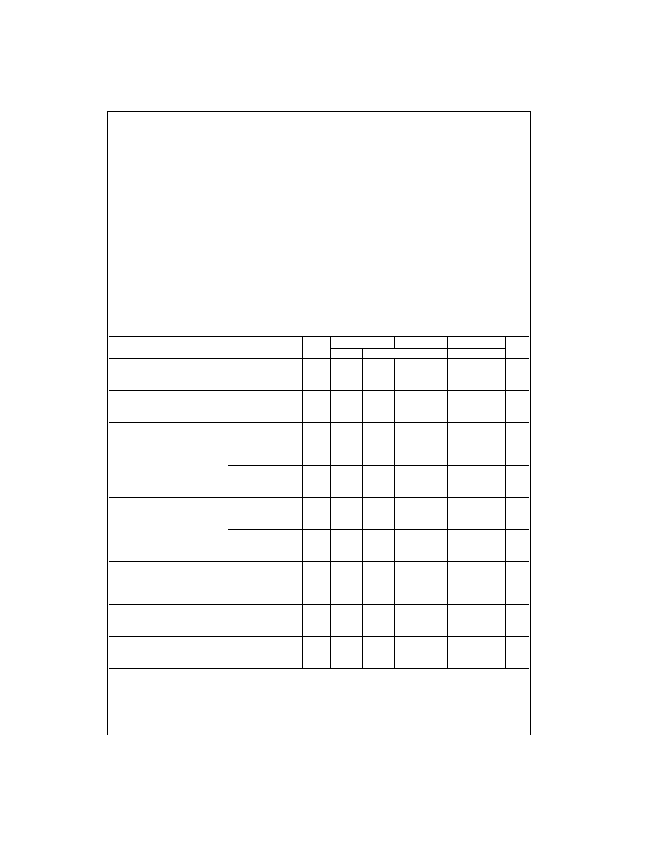
AC Electrical Characteristics
V
CC
=
5V, T
A
=
25
∞
C, C
L
=
15 pF, t
r
=
t
f
=
6 ns
AC Electrical Characteristics
C
L
=
50 pF, t
r
=
t
f
=
6 ns (unless otherwise specified)
Clear
A
B
1.
H
L
H
2.
H
H
H
3.
H
L
H
Symbol
Parameter
Conditions
Typ
Limit
Units
t
PLH
Maximum Propagation Delay A, or B to Q
23
45
ns
t
PHL
Maximum Propagation Delay A, or B to Q
26
50
ns
t
PHL
Maximum Propagation Delay Clear to Q
23
45
ns
t
PLH
Maximum Propagation Delay Clear to Q
26
50
ns
t
W
Minimum Pulse Width A, B or Clear
10
16
ns
Symbol
Parameter
Conditions
V
CC
T
A
=
25
∞
C
T
A
=-
40 to 85
∞
C T
A
=
-
55 to 125
∞
C
Units
Typ
Guaranteed Limits
t
PLH
Maximum Propagation
2.0V
100
250
315
373
ns
Delay A, or B to Q
4.5V
25
50
63
75
ns
6.0V
21
43
54
63
ns
t
PHL
Maximum Propagation
2.0V
110
275
347
410
ns
Delay A, or B to Q
4.5V
28
55
69
82
ns
6.0V
23
47
59
70
ns
t
PHL
Maximum Propagation
2.0V
100
250
315
373
ns
Delay Clear to Q
4.5V
25
50
63
75
ns
6.0V
21
43
54
63
ns
t
PLH
Maximum Propagation
2.0V
110
275
347
410
ns
Delay Clear to Q
4.5V
28
55
69
82
ns
6.0V
23
47
59
70
ns
t
TLH
, t
THL
Maximum Output
2.0V
30
75
95
110
ns
Rise and Fall
4.5V
10
15
19
22
ns
Time
6.0V
8
13
16
19
ns
t
r
, t
f
Maximum Input
2.0V
1000
1000
1000
ns
Rise and Fall
4.5V
500
500
500
ns
Time (Reset only)
6.0V
400
400
400
ns
t
W
Minimum Pulse Width
2.0V
80
101
119
ns
A, B, Clear
4.5V
16
20
24
ns
6.0V
14
17
20
ns
t
REC
Minimum Recovery
2.0V
-
5
0
0
0
ns
Time, Clear
4.5V
0
0
0
ns
Inactive to A or B
6.0V
0
0
0
ns
t
WQ
Output Pulse Width
C
X
=
12 pF
Min
3.0V
283
190
ns
R
X
=
1 k
5.0V
147
120
ns
Max
3.0V
283
400
ns
5.0V
147
185
ns
t
WQ
Output Pulse Width
C
X
=
100 pF
Min
3.0V
1.2
µ
s
R
X
=
10 k
5.0V
1.0
µ
s
Max
3.0V
1.2
µ
s
5.0V
1.0
µ
s

7
www.fairchildsemi.com
MM74HC4538
AC Electrical Characteristics
(Continued)
Note 6: C
PD
determines the no load dynamic consumption, P
D
=
C
PD
V
CC
2
f
+
I
CC
V
CC
, and the no load dynamic current consumption, I
S
=
V
CC
f
+
I
CC
.
Symbol
Parameter
Conditions
V
CC
T
A
=
25
∞
C
T
A
=-
40 to 85
∞
C T
A
=
-
55 to 125
∞
C
Units
Typ
Guaranteed Limits
t
WQ
Output Pulse Width
C
X
=
1000 pF
Min
3.0V
10.5
9.4
µ
s
R
X
=
10 k
5.0V
10.0
9.3
µ
s
Max
3.0V
10.5
11.6
µ
s
5.0V
10.0
10.7
µ
s
t
WQ
Output Pulse Width
C
X
=
0.1
µ
F
Min
5.0V
0.63
0.602
0.595
ms
R
X
=
10k
Max
5.0V
0.77
0.798
0.805
ms
C
IN
Maximum Input
25
pF
Capacitance (Pins 2 & 14)
C
IN
Maximum Input
5
10
10
10
pF
Capacitance (other inputs)
C
PD
Power Dissipation
(per one shot)
150
pF
Capacitance (Note 6)
t
WQ
Pulse Width Match
Between Circuits in
±
1
%
Same Package
www.fairchildsemi.com
8
M
M
74HC4538
Physical Dimensions
inches (millimeters) unless otherwise noted
16-Lead Small Outline Integrated Circuit (SOIC), JEDEC MS-012, 0.150 Narrow
Package Number M16A

9
www.fairchildsemi.com
MM74HC4538
Physical Dimensions
inches (millimeters) unless otherwise noted (Continued)
16-Lead Small Outline Package (SOP), EIAJ TYPE II, 5.3mm Wide
Package Number M16D

www.fairchildsemi.com
10
MM74HC4538 Dual Retr
igger
abl
e
Monost
able Mult
iv
ibr
a
tor
Physical Dimensions
inches (millimeters) unless otherwise noted (Continued)
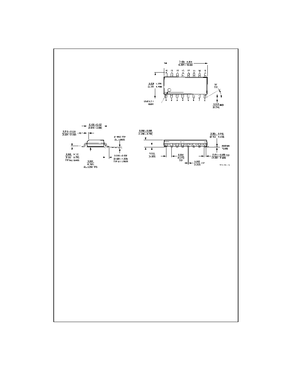
16-Lead Plastic Dual-In-Line Package (PDIP), JEDEC MS-001, 0.300 Wide
Package Number N16E
Fairchild does not assume any responsibility for use of any circuitry described, no circuit patent licenses are implied and
Fairchild reserves the right at any time without notice to change said circuitry and specifications.
LIFE SUPPORT POLICY
FAIRCHILD'S PRODUCTS ARE NOT AUTHORIZED FOR USE AS CRITICAL COMPONENTS IN LIFE SUPPORT
DEVICES OR SYSTEMS WITHOUT THE EXPRESS WRITTEN APPROVAL OF THE PRESIDENT OF FAIRCHILD
SEMICONDUCTOR CORPORATION. As used herein:
1. Life support devices or systems are devices or systems
which, (a) are intended for surgical implant into the
body, or (b) support or sustain life, and (c) whose failure
to perform when properly used in accordance with
instructions for use provided in the labeling, can be rea-
sonably expected to result in a significant injury to the
user.
2. A critical component in any component of a life support
device or system whose failure to perform can be rea-
sonably expected to cause the failure of the life support
device or system, or to affect its safety or effectiveness.
www.fairchildsemi.com