 | –≠–ª–µ–∫—Ç—Ä–æ–Ω–Ω—ã–π –∫–æ–º–ø–æ–Ω–µ–Ω—Ç: NC7S00 | –°–∫–∞—á–∞—Ç—å:  PDF PDF  ZIP ZIP |
© 2000 Fairchild Semiconductor Corporation
DS012138
www.fairchildsemi.com
October 1995
Revised June 2000
NC7S00 T
i
nyLo
gic
HS
2-
Inpu
t N
AND G
a
te
NC7S00
TinyLogic
HS 2-Input NAND Gate
General Description
The NC7S00 is a single 2-Input high performance CMOS
NAND Gate. Advanced Silicon Gate CMOS fabrication
assures high speed and low power circuit operation over a
broad V
CC
range. ESD protection diodes inherently guard
both inputs and output with respect to the V
CC
and GND
rails. Three stages of gain between inputs and output
assures high noise immunity and reduced sensitivity to
input edge rate.
Features
s
Space saving SOT23 or SC70 5-lead package
s
High speed: t
PD
3.5 ns typ
s
Low Quiescent Power: I
CC
<
1
µ
A
s
Balanced Output Drive: 2 mA I
OL
,
-
2 mA I
OH
s
Broad V
CC
Operating Range: 2V
-
6V
s
Balanced Propagation Delays
s
Specified for 3V operation
Ordering Code:
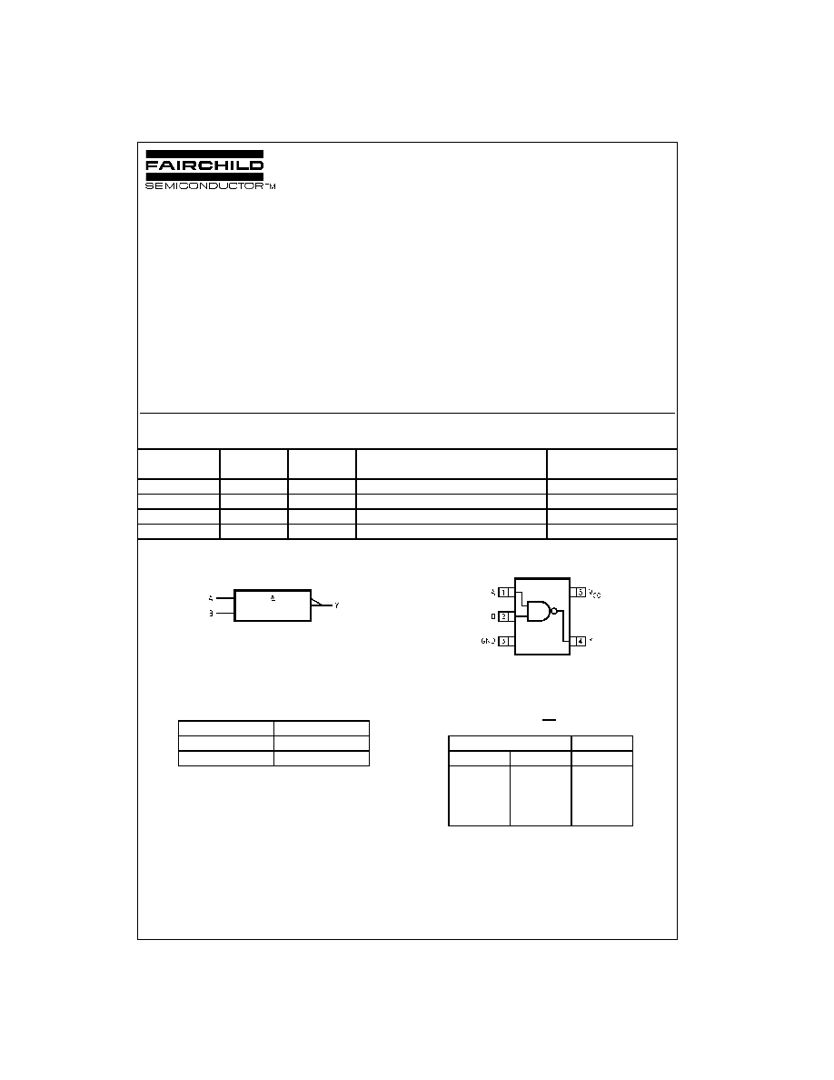
Logic Symbol
IEEE/IEC
Connection Diagram
(Top View)
Pin Descriptions
Function Table
H
=
HIGH Logic Level
L
=
LOW Logic Level
TinyLogic
is a trademark of Fairchild Semiconductor Corporation.
Order Number
Package Product
Code
Package Description
Supplied As
Number
Top Mark
NC7S00M5
MA05B
7S00
5-Lead SOT23, JEDEC MO-178, 1.6mm
250 Units on Tape and Reel
NC7S00M5X
MA05B
7S00
5-Lead SOT23, JEDEC MO-178, 1.6mm
3k Units on Tape and Reel
NC7S00P5
MAA05A
S00
5-Lead SC70, EIAJ SC-88a, 1.25mm Wide
250 Units on Tape and Reel
NC7S00P5X
MAA05A
S00
5-Lead SC70, EIAJ SC-88a, 1.25mm Wide
3k Units on Tape and Reel
Pin Names
Description
A, B
Input
Y
Output
Y
=
AB
Inputs
Output
A
B
Y
L
L
H
L
H
H
H
L
H
H
H
L
www.fairchildsemi.com
2
N
C
7S00
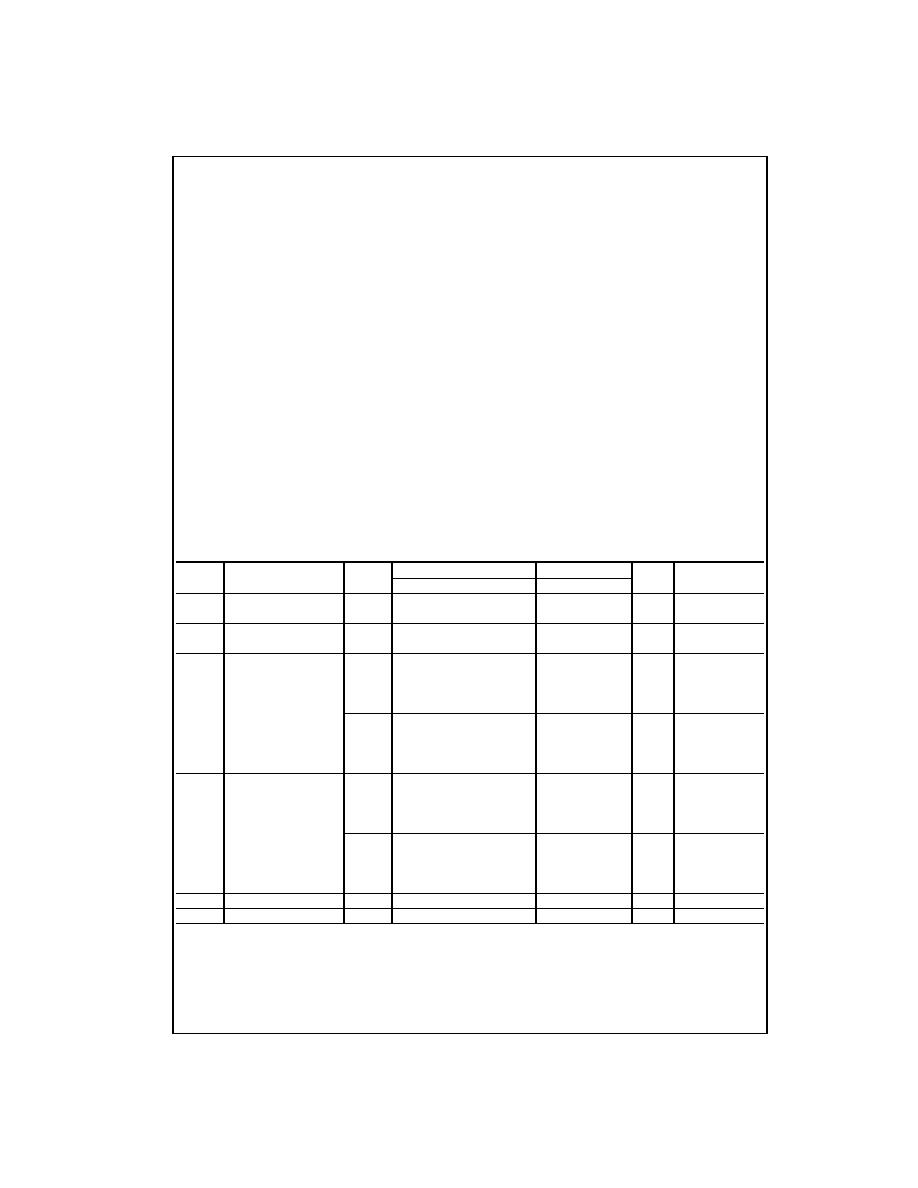
Absolute Maximum Ratings
(Note 1)
Recommended Operating
Conditions
(Note 2)
Note 1: Absolute maximum ratings are those values beyond which damage
to the device may occur. The databook specifications should be met, with-
out exception, to ensure that the system design is reliable over its power
supply, temperature, and output/input loading variables. Fairchild does not
recommend operation of circuits outside the databook specifications.
Note 2: Unused inputs must be held HIGH or LOW. They may not float.
DC Electrical Characteristics
Supply Voltage (V
CC
)
-
0.5V to
+
7.0V
DC Input Diode Current (I
IK
)
@V
IN
-
0.5V
-
20 mA
@V
IN
V
CC
+
0.5V
+
20 mA
DC Input Voltage (V
IN
)
-
0.5V to V
CC
+
0.5V
DC Output Diode Current (I
OK
)
@V
OUT
<
-
0.5V
-
20 mA
@V
OUT
>
V
CC
+
0.5V
+
20 mA
DC Output Voltage (V
OUT
)
-
0.5V to V
CC
+
0.5V
DC Output Source
or Sink Current (I
OUT
)
±
12.5 mA
DC V
CC
or Ground Current
per Output Pin (I
CC
or I
GND
)
±
25 mA
Storage Temperature (T
STG
)
-
65
∞
C to
+
150
∞
C
Junction Temperature (T
J
)
150
∞
C
Lead Temperature (T
L
);
(Soldering, 10 seconds)
260
∞
C
Power Dissipation (P
D
) @
+
85
∞
C
SOT23-5
200 mW
SC70-5
150 mW
Supply Voltage (V
CC
)
2.0V
-
6.0V
Input Voltage (V
IN
)
0V
-
V
CC
Output Voltage (V
OUT
)
0V
-
V
CC
Operating Temperature (T
A
)
-
40
∞
C to
+
85
∞
C
Input Rise and Fall Time (t
r
, t
f
)
V
CC
@ 2.0V
0
-
1000 ns
V
CC
@ 3.0V
0
-
750 ns
V
CC
@ 4.5V
0
-
500 ns
V
CC
@ 6.0V
0
-
400 ns
Thermal Resistance (
JA
)
SOT23-5
300
∞
C/W
SC70-5
425
∞
C/W
Symbol
Parameter
V
CC
T
A
= +
25
∞
C
T
A
= -
40
∞
C to
+
85
∞
C
Units
Conditions
(V)
Min
Typ
Max
Min
Max
V
IH
HIGH Level Input Voltage
2.0
1.50
1.50
V
3.0 - 6.0
0.7V
CC
0.7V
CC
V
IL
LOW Level Input Voltage
2.0
0.50
0.50
V
3.0 - 6.0
0.3V
CC
0.3V
CC
V
OH
HIGH Level Output Voltage
2.0
1.90
2.0
1.90
V
3.0
2.90
3.0
2.90
I
OH
=
-
20
µ
A
4.5
4.40
4.5
4.40
V
IN
=
V
IL
6.0
5.90
6.0
5.90
V
V
IN
=
V
IL
3.0
2.68
2.85
2.63
I
OH
=
-
1.3 mA
4.5
4.18
4.35
4.13
I
OH
=
-
2 mA
6.0
5.68
5.85
5.63
I
OH
=
-
2.6 mA
V
OL
LOW Level Output Voltage
2.0
0.0
0.10
0.10
V
3.0
0.0
0.10
0.10
I
OL
=
20
µ
A
4.5
0.0
0.10
0.10
V
IN
=
V
IH
6.0
0.0
0.10
0.10
V
V
IN
=
V
IH
3.0
0.1
0.26
0.33
I
OL
=
1.3 mA
4.5
0.1
0.26
0.33
I
OL
=
2 mA
6.0
0.1
0.26
0.33
I
OL
=
2.6 mA
I
IN
Input Leakage Current
6.0
±
0.1
±
1.0
µ
A
V
IN
=
V
CC
, GND
I
CC
Quiescent Supply Current
6.0
1.0
10.0
µ
A
V
IN
=
V
CC
, GND
3
www.fairchildsemi.com
NC7S00
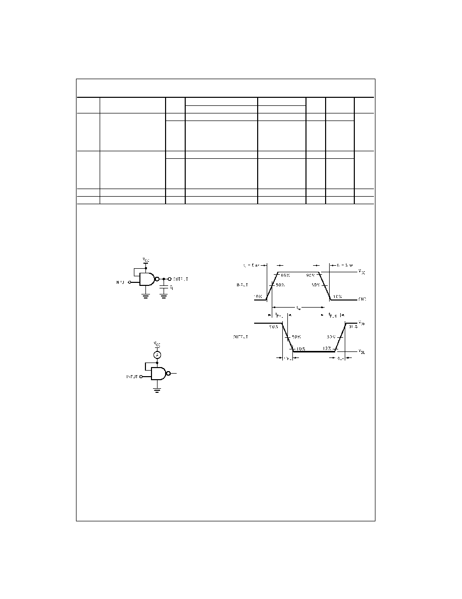
AC Electrical Characteristics
Note 3: C
PD
is defined as the value of the internal equivalent capacitance which is derived from dynamic operating current consumption (I
CCD
) at no output
loading and operating at 50% duty cycle. (See Figure 2.) C
PD
is related to I
CCD
dynamic operating current by the expression:
I
CCD
=
(C
PD
) (V
CC
) (f
IN
)
+
(I
CC
static).
AC Loading and Waveforms
C
L
includes load and stray capacitance
Input PRR
=
1.0 MHz, t
w
=
500 ns
FIGURE 1. AC Test Circuit
Input
=
AC Waveform;
PRR
=
variable; Duty Cycle
=
50%
FIGURE 2. I
CCD
Test Circuit
FIGURE 3. AC Waveforms
Symbol
Parameter
V
CC
T
A
=
+
25
∞
C
T
A
=
-
40
∞
C to
+
85
∞
C
Units
Conditions Fig. No.
(V)
Min
Typ
Max
Min
Max
t
PLH
,
Propagation Delay
5.0
3.5
15
ns
C
L
=
15 pF
Figures
1, 3
t
PHL
2.0
19
100
125
ns
C
L
=
50 pF
3.0
10.5
27
35
4.5
7.5
20
25
6.0
6.5
17
21
t
TLH
,
Output Transition Time
5.0
3.0
10
ns
C
L
=
15 pF
Figures
1, 3
t
THL
2.0
25
125
155
ns
C
L
=
50 pF
3.0
16
35
45
4.5
11
25
31
6.0
9
21
26
C
IN
Input Capacitance
Open
2
10
10
pF
C
PD
Power Dissipation Capacitance
5.0
6
pF
(Note 3)
Figure 2
www.fairchildsemi.com
4
N
C
7S00
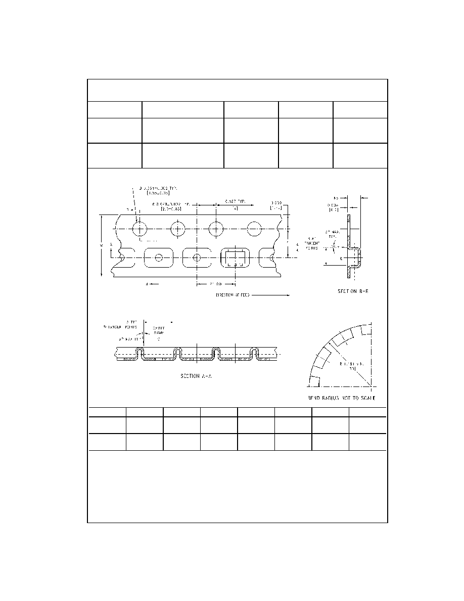
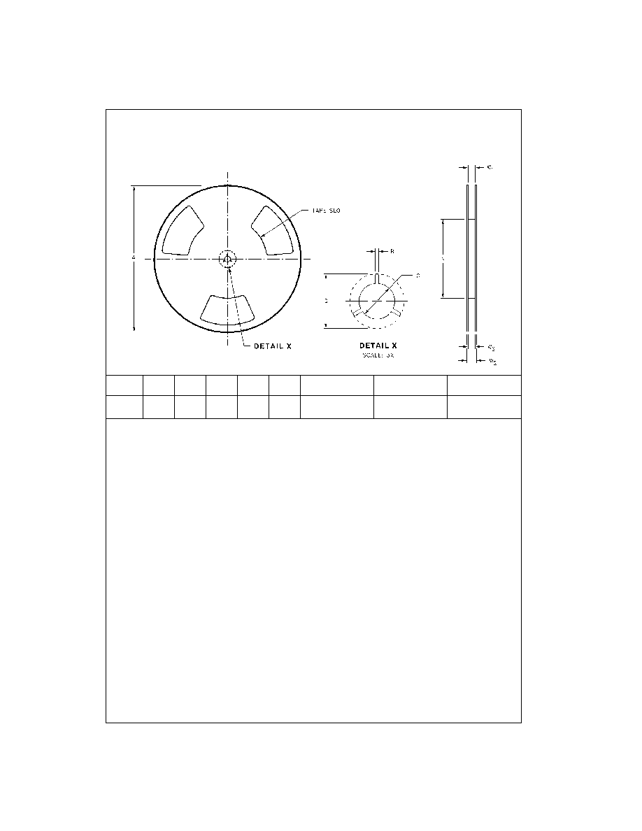
Tape and Reel Specification
TAPE FORMAT
TAPE DIMENSIONS inches (millimeters)
Package
Tape
Number
Cavity
Cover Tape
Designator
Section
Cavities
Status
Status
Leader (Start End)
125 (typ)
Empty
Sealed
M5, P5
Carrier
250
Filled
Sealed
Trailer (Hub End)
75 (typ)
Empty
Sealed
Leader (Start End)
125 (typ)
Empty
Sealed
M5X, P5X
Carrier
3000
Filled
Sealed
Trailer (Hub End)
75 (typ)
Empty
Sealed
Package
Tape Size
DIM A
DIM B
DIM F
DIM K
o
DIM P1
DIM W
SC70-5
8 mm
0.093
0.096
0.138
±
0.004
0.053
±
0.004
0.157
0.315
±
0.004
(2.35)
(2.45)
(3.5
±
0.10)
(1.35
±
0.10)
(4)
(8
±
0.1)
SOT23-5
8 mm
0.130
0.130
0.138
±
0.002
0.055
±
0.004
0.157
0.315
±
0.012
(3.3)
(3.3)
(3.5
±
0.05)
(1.4
±
0.11)
(4)
(8
±
0.3)
5
www.fairchildsemi.com
NC7S00
Tape and Reel Specification
(Continued)
REEL DIMENSIONS inches (millimeters)
Tape
Size
A
B
C
D
N
W1
W2
W3
8 mm
7.0
0.059
0.512
0.795
2.165
0.331
+
0.059/
-
0.000
0.567
W1
+
0.078/
-
0.039
(177.8)
(1.50)
(13.00)
(20.20)
(55.00)
(8.40
+
1.50/
-
0.00)
(14.40)
(W1
+
2.00/
-
1.00)

www.fairchildsemi.com
6
N
C
7S00
Physical Dimensions
inches (millimeters) unless otherwise noted
5-Lead SOT23, JEDEC MO-178, 1.6mm
Package Number MA05B
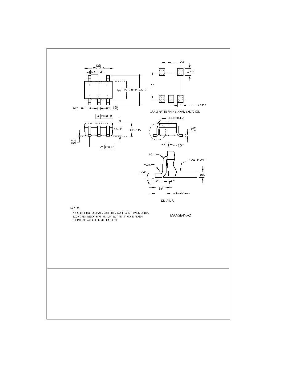
7
www.fairchildsemi.com
NC7S00 T
i
nyLo
gic
HS
2-
Inpu
t N
AND G
a
te
Physical Dimensions
inches (millimeters) unless otherwise noted (Continued)
5-Lead SC70, EIAJ SC-88a, 1.25mm Wide
Package Number MAA05A
Fairchild does not assume any responsibility for use of any circuitry described, no circuit patent licenses are implied and
Fairchild reserves the right at any time without notice to change said circuitry and specifications.
LIFE SUPPORT POLICY
FAIRCHILD'S PRODUCTS ARE NOT AUTHORIZED FOR USE AS CRITICAL COMPONENTS IN LIFE SUPPORT
DEVICES OR SYSTEMS WITHOUT THE EXPRESS WRITTEN APPROVAL OF THE PRESIDENT OF FAIRCHILD
SEMICONDUCTOR CORPORATION. As used herein:
1. Life support devices or systems are devices or systems
which, (a) are intended for surgical implant into the
body, or (b) support or sustain life, and (c) whose failure
to perform when properly used in accordance with
instructions for use provided in the labeling, can be rea-
sonably expected to result in a significant injury to the
user.
2. A critical component in any component of a life support
device or system whose failure to perform can be rea-
sonably expected to cause the failure of the life support
device or system, or to affect its safety or effectiveness.
www.fairchildsemi.com