© 2000 Fairchild Semiconductor Corporation
DS012185
www.fairchildsemi.com
February 1997
Revised June 2000
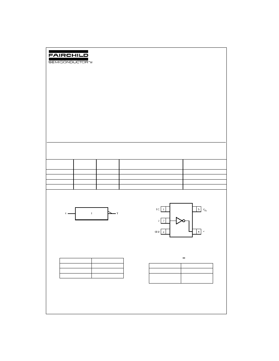
NC7ST04
T
i
nyL
ogic
H
S
T
In
v
e
r
te
r
NC7ST04
TinyLogic
HST Inverter
General Description
The NC7ST04 is a single high performance CMOS
Inverter, with TTL-compatible inputs. Advanced Silicon
Gate CMOS fabrication assures high speed and low power
circuit operation. ESD protection diodes inherently guard
both input and output with respect to the V
CC
and GND
rails. High gain circuitry offers high noise immunity and
reduced sensitivity to input edge rate. The TTL-compatible
input facilitates TTL to NMOS/CMOS interfacing. Device
performance is similar to MM74HCT but with Ω the output
current drive of HC/HCT.
Features
s
Space saving SOT23 or SC70 5-lead package
s
High Speed; t
PD
<
7 ns typ, V
CC
=
5V, C
L
=
15 pF
s
Low Quiescent Power; I
CC
<
1
µ
A typ, V
CC
=
5.5V
s
Balanced Output Drive; 2 mA I
OL
,
-
2 mA I
OH
s
TTL-compatible inputs
Ordering Code:
Logic Symbol
IEEE/IEC
Connection Diagram
(Top View)
Pin Descriptions
Function Table
H
=
HIGH Logic Level
L
=
LOW Logic Level
TinyLogic
is a trademark of Fairchild Semiconductor Corporation.
Order Package
Product
Code
Package Description
Supplied As
Number
Number
Top Mark
NC7ST04M5
MA05B
8S04
5-Lead SOT23, JEDEC MO-178, 1.6mm
250 Units on Tape and Reel
NC7ST04M5X
MA05B
8S04
5-Lead SOT23, JEDEC MO-178, 1.6mm
3k Units on Tape and Reel
NC7ST04P5
MAA05A
T04
5-Lead SC70, EIAJ SC-88a, 1.25mm Wide
250 Units on Tape and Reel
NC7ST04P5X
MAA05A
T04
5-Lead SC70, EIAJ SC-88a, 1.25mm Wide
3k Units on Tape and Reel
Pin Names
Description
A
Input
Y
Output
NC
No Connect
Y
=
A
Input
Output
A
Y
L
H
H
L
www.fairchildsemi.com
2
NC7ST04
Absolute Maximum Ratings
(Note 1)
Recommended Operating
Conditions
(Note 2)
Note 1: Absolute Maximum Ratings are those values beyond which dam-
age to the device may occur. The databook specifications should be met,
without exception, to ensure that the system design is reliable over its
power supply, temperature, and output/input loading variables. Fairchild
does not recommend operation of circuits outside the databook specifica-
tions.
Note 2: Unused inputs must be held HIGH or LOW. They may not float.
DC Electrical Characteristics
Supply Voltage (V
CC
)
-
0.5V to
+
7.0V
DC Input Diode Current (I
IK
)
V
IN
<
-
0.5V
-
20 mA
V
IN
V
CC
+
0.5V
+
20 mA
DC Input Voltage (V
IN
)
-
0.5V to V
CC
+
0.5V
DC Output Diode Current (I
OK
)
V
OUT
<
-
0.5V
-
20 mA
V
OUT
>
V
CC
+
0.5V
+
20 mA
Output Voltage (V
OUT
)
-
0.5V to V
CC
+
0.5V
DC Output Source or Sink
Current (I
OUT
)
±
12.5 mA
DC V
CC
or Ground Current per
Supply Pin (I
CC
or I
GND
)
±
25 mA
Storage Temperature (T
STG
)
-
65
∞
C to
+
150
∞
C
Junction Temperature (T
J
)
150
∞
C
DC V
CC
or Ground Current per
(Soldering, 10 seconds)
260
∞
C
Power Dissipation (P
D
) @
+
85
∞
C
SOT23-5
200 mW
SC70-5
150 mW
Supply Voltage
4.5V≠5.5V
Input Voltage (V
IN
)
0V≠V
CC
Output Voltage (V
OUT
)
0V≠V
CC
Operating Temperature (T
A
)
-
40
∞
C to
+
85
∞
C
Input Rise and Fall Time (t
r
, t
f
)
V
CC
=
5.0V
0≠500 ns
Thermal Resistance (
JA
)
SOT23-5
300
∞
C/W
SC70-5
425
∞
C/W
Symbol
Parameter
V
CC
T
A
=
+
25
∞
C
T
A
=
-
40
∞
C to
+
85
∞
C
Units
Conditions
(V)
Min
Typ
Max
Min
Max
V
IH
HIGH Level Input Voltage
4.5≠5.5
2.0
2.0
V
V
IL
LOW Level Input Voltage
4.5≠5.5
0.8
0.8
V
V
OH
HIGH Level Output Voltage
4.5
4.4
4.5
4.4
V
I
OH
=
-
20
µ
A, V
IN
=
V
IL
,
4.5
4.18
4.35
4.13
V
I
OH
=
-
2 mA
V
OL
LOW Level Output Voltage
4.5
0
0.1
0.1
V
I
OL
=
20
µ
A, V
IN
=
V
IH
,
4.5
0.10
0.26
0.33
V
I
OL
=
2 mA
I
IN
Input Leakage Current
5.5
±
0.1
±
1.0
µ
A
0
V
IN
5.5V
I
CC
Quiescent Supply Current
5.5
1.0
10.0
µ
A
V
IN
=
V
CC
or GND
I
CCT
I
CC
per Input
5.5
2.0
2.9
mA
Input V
IN
=
0.5V or 2.4V
3
www.fairchildsemi.com
NC7ST04
AC Electrical Characteristics
Note 3: C
PD
is defined as the value of the internal equivalent capacitance which is derived from dynamic operating current consumption (I
CCD
) at no output
loading and operating at 50% duty cycle. (See Figure 2.) C
PD
is related to I
CCD
dynamic operating current by the expression:
I
CCD
=
(C
PD
) (V
CC
) (f
IN
)
+
(I
CCstatic
).
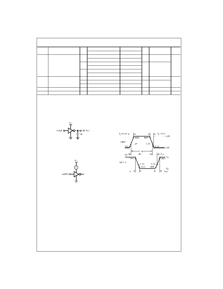
AC Loading and Waveforms
C
L
includes load and stray capacitance
Input PRR
=
1.0 MHz, t
w
=
500 ns
FIGURE 1. AC Test Circuit
Input
=
AC Waveform; PRR
=
Variable; Duty Cycle
=
50%
FIGURE 2. I
CCD
Test Circuit
FIGURE 3. AC Waveforms
Symbol
Parameter
V
CC
T
A
=
+
25
∞
C
T
A
=
-
40
∞
C to
+
85
∞
C
Units
Conditions
Fig. No.
(V)
Min
Typ
Max
Min
Max
t
PLH
,
Propagation Delay
5.0
3.5
12
ns
C
L
=
15 pF
Figures
1, 3
t
PHL
6.0
17
4.5
6.2
16
20
ns
C
L
=
50 pF
11.4
27
31
5.5
4.3
14
18
11.1
26
30
t
TLH
,
Output Transition Time
5.0
4
10
ns
C
L
=
15 pF
Figures
1, 3
t
THL
4.5
11
25
31
ns
C
L
=
50 pF
5.5
10
21
26
C
IN
Input Capacitance
Open
2
10
pF
C
PD
Power Dissipation Capacitance
5.0
6
pF
(Note 3)
Figure 2