 | –≠–ª–µ–∫—Ç—Ä–æ–Ω–Ω—ã–π –∫–æ–º–ø–æ–Ω–µ–Ω—Ç: NDS9430A | –°–∫–∞—á–∞—Ç—å:  PDF PDF  ZIP ZIP |
December 1997
NDS9430A
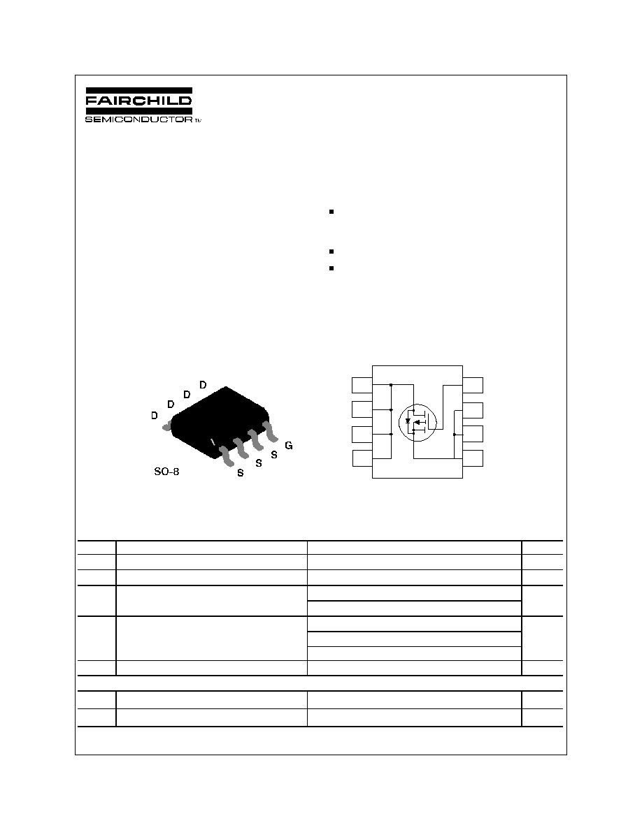
Single P-Channel Enhancement Mode Field Effect Transistor
General Description
Features
___________________________________________________________________________________________
Absolute Maximum Ratings
T
A
= 25∞C unless otherwise noted
Symbol
Parameter
NDS9430A
Units
V
DSS
Drain-Source Voltage
-20
V
V
GSS
Gate-Source Voltage
± 20
V
I
D
Drain Current - Continuous
(Note 1a)
± 5.3
A
- Pulsed
± 20
P
D
Maximum Power Dissipation
(Note 1a)
2.5
W
(Note 1b)
1.2
(Note 1c)
1
T
J
,T
STG
Operating and Storage Temperature Range
-55 to 150
∞C
THERMAL CHARACTERISTICS
R
JA
Thermal Resistance, Junction-to-Ambient
(Note 1a)
50
∞C/W
R
JC
Thermal Resistance, Junction-to-Case
(Note 1)
25
∞C/W
NDS9430A Rev.A
These P-Channel enhancement mode power field effect
transistors are produced using National's proprietary, high cell
density, DMOS technology. This very high density process is
especially tailored to minimize on-state resistance, provide
superior switching performance, and withstand high energy
pulses in the avalanche and commutation modes. These
devices are particularly suited for low voltage applications such
as notebook computer power management and other battery
powered circuits where fast switching, low in-line power loss,
and resistance to transients are needed.
-5.3A, -20V. R
DS(ON)
= 0.05
@ V
GS
= -10V
R
DS(ON)
= 0.065
@ V
GS
= -6V
R
DS(ON)
= 0.09
@ V
GS
= -4.5V.
High density cell design for extremely low R
DS(ON).
High power and current handling capability in a widely used
surface mount package.
5
6
7
8
4
3
2
1
© 1997 Fairchild Semiconductor Corporation
Electrical Characteristics
(T
A
= 25∞C unless otherwise noted)
Symbol
Parameter
Conditions
Min
Typ
Max
Units
OFF CHARACTERISTICS
BV
DSS
Drain-Source Breakdown Voltage
V
GS
= 0 V, I
D
= -250 µA
-20
V
I
DSS
Zero Gate Voltage Drain Current
V
DS
= -16 V, V
GS
= 0 V
-1
µA
V
DS
= -10 V, V
GS
= 0 V
T
J
= 70∞C
-5
µA
I
GSSF
Gate - Body Leakage, Forward
V
GS
= 20 V, V
DS
= 0 V
100
nA
I
GSSR
Gate - Body Leakage, Reverse
V
GS
= -20 V, V
DS
= 0 V
-100
nA
ON CHARACTERISTICS
(Note 2)
V
GS(th)
Gate Threshold Voltage
V
DS
= V
GS
, I
D
= -250 µA
-1
-1.4
-3
V
T
J
= 125∞C
-0.7
-1
-2
R
DS(ON)
Static Drain-Source On-Resistance
V
GS
= -10 V, I
D
= -5.3 A
0.038
0.05
T
J
= 125∞C
0.054
0.1
V
GS
= -6 V, I
D
= -4.7 A
0.046
0.065
V
GS
= -4.5 V, I
D
= -4.2 A
0.064
0.09
I
D(on)
On-State Drain Current
V
GS
= -10 V, V
DS
= -5 V
-15
A
V
GS
= -4.5, V
DS
= -5V
-3.6
g
FS
Forward Transconductance
V
DS
= 15 V, I
D
= 5.3 A
10
S
DYNAMIC CHARACTERISTICS
C
iss
Input Capacitance
V
DS
= 15 V, V
GS
= 0 V,
f = 1.0 MHz
950
pF
C
oss
Output Capacitance
610
pF
C
rss
Reverse Transfer Capacitance
220
pF
SWITCHING CHARACTERISTICS
(Note 2)
t
D(on)
Turn - On Delay Time
V
DD
= -10 V, I
D
= -1 A,
V
GEN
= -10 V, R
GEN
= 6
10
30
ns
t
r
Turn - On Rise Time
18
60
ns
t
D(off)
Turn - Off Delay Time
80
120
ns
t
f
Turn - Off Fall Time
45
100
ns
Q
g
Total Gate Charge
V
DS
= -10 V,
I
D
= -5.3 A, V
GS
= -10 V
29
50
nC
Q
gs
Gate-Source Charge
3
nC
Q
gd
Gate-Drain Charge
9
nC
NDS9430A Rev.A
Electrical Characteristics
(T
A
= 25∞C unless otherwise noted)
Symbol
Parameter
Conditions
Min
Typ
Max
Units
DRAIN-SOURCE DIODE CHARACTERISTICS AND MAXIMUM RATINGS
I
S
Maximum Continuous Drain-Source Diode Forward Current
-2.1
A
V
SD
Drain-Source Diode Forward Voltage
V
GS
= 0 V, I
S
= -2.4 A
(Note 2)
-0.85
-1.2
V
t
rr
Reverse Recovery Time
V
GS
= 0V, I
F
= -2.4 A, dI
F
/dt = 100 A/µs
100
ns
Notes:
1. R
JA
is the sum of the junction-to-case and case-to-ambient thermal resistance where the case thermal reference is defined as the solder mounting surface of the drain pins. R
JC
is guaranteed by
design while R
CA
is determined by the user's board design.
P
D
(
t
) =
T
J
-
T
A
R
J A
(
t
)
=
T
J
-
T
A
R
J C
+
R
CA
(
t
)
=
I
D
2
(
t
) ◊
R
DS
(
ON
)
T
J
Typical R
JA
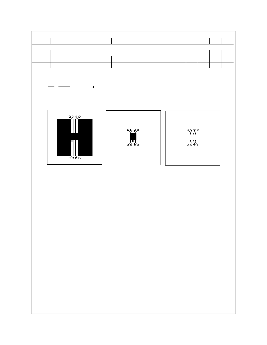
using the board layouts shown below on 4.5"x5" FR-4 PCB in a still air environment:
a. 50
o
C/W when mounted on a 1 in
2
pad of 2oz cpper.
b. 105
o
C/W when mounted on a 0.04 in
2
pad of 2oz cpper.
c. 125
o
C/W when mounted on a 0.006 in
2
pad of 2oz cpper.
Scale 1 : 1 on letter size paper
2. Pulse Test: Pulse Width < 300µs, Duty Cycle < 2.0%.
NDS9430A Rev.A
1a
1b
1c
NDS9430A Rev.A
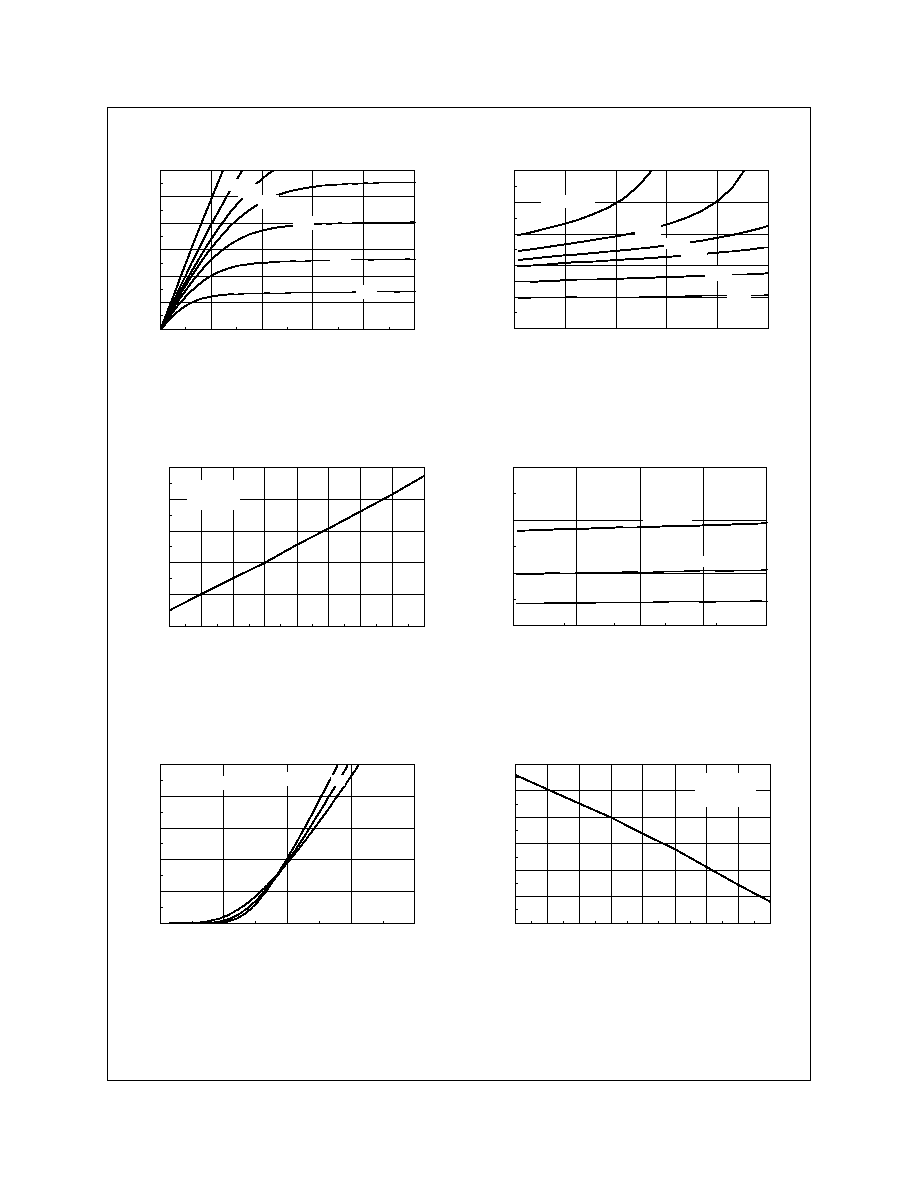
-5
-4
-3
-2
-1
0
-30
-25
-20
-15
-10
-5
0
V , DRAIN-SOURCE VOLTAGE (V)
I , DRAIN-SOURCE CURRENT (A)
-6.0
-4.0
V =-10V
GS
DS
D
-3.0
-4.5
-3.5
-5.0
-20
-16
-12
-8
-4
0
0.5
1
1.5
2
2.5
3
I , DRAIN CURRENT (A)
DRAIN-SOURCE ON-RESISTANCE
V = -3.5V
GS
D
R , NORMALIZED
DS(on)
-6.0V
-10V
-6.0V
-5.0V
-4.0V
-4.5V
Figure 1. On-Region Characteristics
Figure 2. On-Resistance Variation
with Drain Current and Gate Voltage
Typical Electrical Characteristics
-50
-25
0
2 5
5 0
7 5
100
125
150
0.6
0.8
1
1.2
1.4
1.6
T , JUNCTION TEMPERATURE (∞C)
DRAIN-SOURCE ON-RESISTANCE
J
V = -10V
GS
I = -5.3A
D
R
,
N
O
R
M
A
L
I
Z
E
D
D
S
(
O
N
)
-20
-15
-10
-5
0
0.5
1
1.5
2
I , DRAIN CURRENT (A)
DRAIN-SOURCE ON-RESISTANCE
D
R , NORMALIZED
DS(on)
25∞C
-55∞C
V = -10V
GS
T = 125∞C
J
Figure 3. On-Resistance Variation
with Temperature
Figure 4. On-Resistance Variation
with Drain Current and Temperature
-5
-4
-3
-2
-1
-20
-16
-12
-8
-4
0
-V , GATE TO SOURCE VOLTAGE (V)
-I , DRAIN CURRENT (A)
25
125
V = -10V
DS
GS
D
T = -55∞C
J
-50
-25
0
25
50
75
100
125
150
0.6
0.7
0.8
0.9
1
1.1
1.2
T , JUNCTION TEMPERATURE (∞C)
GATE-SOURCE THRESHOLD VOLTAGE
I = -250µA
D
V = V
DS
GS
J
V , NORMALIZED
th
Figure 5. Transfer Characteristics
Figure 6. Gate Threshold Variation
with Temperature
NDS9430A Rev.A
-50
-25
0
25
50
75
100
125
150
0.94
0.96
0.98
1
1.02
1.04
1.06
1.08
1.1
T , JUNCTION TEMPERATURE (∞C)
DRAIN-SOURCE BREAKDOWN VOLTAGE
I = -250µA
D
BV , NORMALIZED
DSS
J
0
0.3
0.6
0.9
1.2
1.5
0.001
0.01
0.1
1
5
10
20
-V , BODY DIODE FORWARD VOLTAGE (V)
-I , REVERSE DRAIN CURRENT (A)
T = 125∞C
J
25∞C
-55∞C
V = 0V
GS
SD
S
Figure 7. Breakdown Voltage
Variation with Temperature
Figure 8. Body Diode Forward Voltage Variation
with Source Current and
Temperature
Typical Electrical Characteristics
(continued)
0
10
20
30
40
0
2
4
6
8
10
Q , GATE CHARGE (nC)
-V , GATE-SOURCE VOLTAGE (V)
g
GS
I = -5.3A
D
V = -10V
DS
-15V
-20V
0.1
0.3
1
3
10
30
1 0 0
2 0 0
3 0 0
5 0 0
1 0 0 0
2 0 0 0
3 0 0 0
-V , DRAIN TO SOURCE VOLTAGE (V)
CAPACITANCE (pF)
DS
C iss
f = 1 MHz
V = 0V
GS
C oss
C rss
D
S
-V
DD
R
L
V
OUT
V
GS
DUT
V
IN
R
GEN
G
10%
50%
90%
10%
90%
90%
50%
V
IN
V
OUT
o n
off
d(off)
f
r
d(on)
t
t
t
t
t
t
INVERTED
10%
PULSE W IDTH
Figure 9. Capacitance Characteristics
Figure 10. Gate Charge Characteristics
Figure 11. Switching Test Circuit
Figure 12. Switching Waveforms
NDS9430A Rev.A
-20
-15
-10
-5
0
0
4
8
12
16
20
I , DRAIN CURRENT (A)
g
,
T
R
A
N
S
C
O
N
D
U
C
T
A
N
C
E
(
S
I
E
M
E
N
S
)
T = -55∞C
J
25∞C
D
FS
V = -15V
DS
125∞C
Figure 13. Transconductance Variation with Drain
Current and Temperature
Figure 16. Maximum Safe Operating Area
Typical Electrical and Thermal Characteristics
(continued)
0
0.2
0.4
0.6
0.8
1
2
3
4
5
6
2oz COPPER MOUNTING PAD AREA (in )
I , STEADY-STATE DRAIN CURRENT (A)
D
2
1c
1 b
1a
4.5"x5" FR-4 Board
T = 2 5 C
Still Air
V = - 1 0 V
A
o
GS
0
0.2
0.4
0.6
0.8
1
0.5
1
1.5
2
2.5
2oz COPPER MOUNTING PAD AREA (in )
STEADY-STATE POWER DISSIPATION (W)
2
1c
1 b
1a
4.5"x5" FR-4 Board
T = 2 5 C
Still Air
A
o
0.1
0.2
0.5
1
2
5
10
3 0
5 0
0.01
0.03
0.1
0.3
1
3
10
30
- V , DRAIN-SOURCE VOLTAGE (V)
-I , DRAIN CURRENT (A)
DS
D
1s
100ms
10s
DC
10ms
RDS(ON) LIMIT
1ms
V = -10V
SINGLE PULSE
R = See Note 1c
T = 25∞C
GS
A
J A
100us
Figure 14. SO-8 Maximum Steady-State Power
Dissipation versus Copper Mounting Pad
Area.
Figure 15. Maximum Steady-State Drain
Current versus Copper Mounting Pad
Area.
Figure 17. Transient Thermal Response Curve
.
Note: Thermal characterization performed using the conditions described in note 1c. Transient thermal response will change
depending on the circuit board design.
0 .0001
0 .001
0 .0 1
0 .1
1
1 0
1 0 0
3 0 0
0 .0 0 1
0 .0 0 2
0 .0 0 5
0 .0 1
0 .0 2
0 .0 5
0 .1
0 .2
0 .5
1
t , TIME (sec)
TRANSIENT THERMAL RESISTANCE
r(t), NORMALIZED EFFECTIVE
1
Single Pulse
D = 0.5
0.1
0.05
0.02
0.01
0.2
Duty Cycle, D = t / t
1
2
R (t) = r(t) * R
R = See Note 1c
JA
JA
JA
T - T = P * R (t)
JA
A
J
P(pk)
t
1
t
2
DISCLAIMER
FAIRCHILD SEMICONDUCTOR RESERVES THE RIGHT TO MAKE CHANGES WITHOUT FURTHER
NOTICE TO ANY PRODUCTS HEREIN TO IMPROVE RELIABILITY, FUNCTION OR DESIGN. FAIRCHILD
DOES NOT ASSUME ANY LIABILITY ARISING OUT OF THE APPLICATION OR USE OF ANY PRODUCT
OR CIRCUIT DESCRIBED HEREIN; NEITHER DOES IT CONVEY ANY LICENSE UNDER ITS PATENT
RIGHTS, NOR THE RIGHTS OF OTHERS.
TRADEMARKS
The following are registered and unregistered trademarks Fairchild Semiconductor owns or is authorized to use and is
not intended to be an exhaustive list of all such trademarks.
LIFE SUPPORT POLICY
FAIRCHILD'S PRODUCTS ARE NOT AUTHORIZED FOR USE AS CRITICAL COMPONENTS IN LIFE SUPPORT
DEVICES OR SYSTEMS WITHOUT THE EXPRESS WRITTEN APPROVAL OF FAIRCHILD SEMICONDUCTOR CORPORATION.
As used herein:
1. Life support devices or systems are devices or
systems which, (a) are intended for surgical implant into
the body, or (b) support or sustain life, or (c) whose
failure to perform when properly used in accordance
with instructions for use provided in the labeling, can be
reasonably expected to result in significant injury to the
user.
2. A critical component is any component of a life
support device or system whose failure to perform can
be reasonably expected to cause the failure of the life
support device or system, or to affect its safety or
effectiveness.
PRODUCT STATUS DEFINITIONS
Definition of Terms
Datasheet Identification
Product Status
Definition
Advance Information
Preliminary
No Identification Needed
Obsolete
This datasheet contains the design specifications for
product development. Specifications may change in
any manner without notice.
This datasheet contains preliminary data, and
supplementary data will be published at a later date.
Fairchild Semiconductor reserves the right to make
changes at any time without notice in order to improve
design.
This datasheet contains final specifications. Fairchild
Semiconductor reserves the right to make changes at
any time without notice in order to improve design.
This datasheet contains specifications on a product
that has been discontinued by Fairchild semiconductor.
The datasheet is printed for reference information only.
Formative or
In Design
First Production
Full Production
Not In Production
OPTOLOGICTM
OPTOPLANARTM
PACMANTM
POPTM
Power247TM
PowerTrench
QFETTM
QSTM
QT OptoelectronicsTM
Quiet SeriesTM
SILENT SWITCHER
FAST
FASTrTM
FRFETTM
GlobalOptoisolatorTM
GTOTM
HiSeCTM
ISOPLANARTM
LittleFETTM
MicroFETTM
MicroPakTM
MICROWIRETM
Rev. H4
Æ
ACExTM
BottomlessTM
CoolFETTM
CROSSVOLT
TM
DenseTrenchTM
DOMETM
EcoSPARKTM
E
2
CMOS
TM
EnSigna
TM
FACTTM
FACT Quiet SeriesTM
SMART STARTTM
STAR*POWERTM
StealthTM
SuperSOTTM-3
SuperSOTTM-6
SuperSOTTM-8
SyncFETTM
TinyLogicTM
TruTranslationTM
UHCTM
UltraFET
Æ
Æ
Æ
STAR*POWER is used under license
VCXTM