 | –≠–ª–µ–∫—Ç—Ä–æ–Ω–Ω—ã–π –∫–æ–º–ø–æ–Ω–µ–Ω—Ç: RFP50N06 | –°–∫–∞—á–∞—Ç—å:  PDF PDF  ZIP ZIP |
©2002 Fairchild Semiconductor Corporation
RFG50N06, RFP50N06, RF1S50N06SM Rev. B
RFG50N06, RFP50N06, RF1S50N06SM
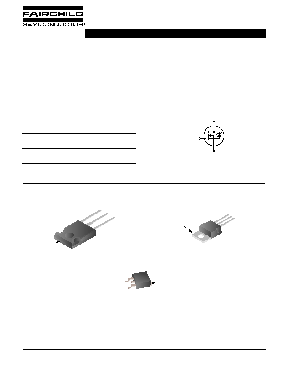
50A, 60V, 0.022 Ohm, N-Channel Power
MOSFETs
These N-Channel power MOSFETs are manufactured using
the MegaFET process. This process, which uses feature
sizes approaching those of LSI integrated circuits gives
optimum utilization of silicon, resulting in outstanding
performance. They were designed for use in applications
such as switching regulators, switching converters, motor
drivers, and relay drivers. These transistors can be operated
directly from integrated circuits.
Formerly developmental type TA49018.
Features
∑ 50A, 60V
∑ r
DS(ON)
= 0.022
∑ Temperature Compensating PSPICE
Æ
Model
∑ Peak Current vs Pulse Width Curve
∑ UIS Rating Curve
∑ 175
o
C Operating Temperature
Symbol
Packaging
Ordering Information
PART NUMBER
PACKAGE
BRAND
RFG50N06
TO-247
RFG50N06
RFP50N06
TO-220AB
RFP50N06
RF1S50N06SM
TO-263AB
F1S50N06
NOTE: When ordering, use the entire part number. Add the suffix, 9A,
to obtain the TO-263AB variant in tape and reel, i.e. RF1S50N06SM9A.
G
D
S
JEDEC STYLE TO-247
JEDEC TO-220AB
JEDEC TO-263AB
DRAIN
(BOTTOM
SIDE METAL)
SOURCE
DRAIN
GATE
DRAIN
(FLANGE)
SOURCE
DRAIN
GATE
DRAIN
(FLANGE)
GATE
SOURCE
Data Sheet
January 2002
©2002 Fairchild Semiconductor Corporation
RFG50N06, RFP50N06, RF1S50N06SM Rev. B
Absolute Maximum Ratings
T
C
= 25
o
C, Unless Otherwise Specified
RFG50N06, RFP50N06
RF1S50N06SM
UNITS
Drain to Source Voltage (Note 1) . . . . . . . . . . . . . . . . . . . . . . . . . . . . . . . . . . . . . V
DSS
60
V
Drain to Gate Voltage (R
GS
= 20k
) (Note 1) . . . . . . . . . . . . . . . . . . . . . . . . . . V
DGR
60
V
Gate to Source Voltage . . . . . . . . . . . . . . . . . . . . . . . . . . . . . . . . . . . . . . . . . . . . . V
GS
±
20
V
Continuous Drain Current (Figure 2) . . . . . . . . . . . . . . . . . . . . . . . . . . . . . . . . . . . . .I
D
Pulsed Drain Current . . . . . . . . . . . . . . . . . . . . . . . . . . . . . . . . . . . . . . . . . . . . . I
DM
50
(Figure 5)
A
Pulsed Avalanche Rating . . . . . . . . . . . . . . . . . . . . . . . . . . . . . . . . . . . . . . . . . . . . E
AS
(Figure 6)
Power Dissipation . . . . . . . . . . . . . . . . . . . . . . . . . . . . . . . . . . . . . . . . . . . . . . . . . . P
D
Linear Derating Factor . . . . . . . . . . . . . . . . . . . . . . . . . . . . . . . . . . . . . . . . . . . . . . .
131
0.877
W
W/
o
C
Operating and Storage Temperature . . . . . . . . . . . . . . . . . . . . . . . . . . . . . . . T
J
, T
STG
-55 to 175
o
C
Maximum Temperature for Soldering
Leads at 0.063in (1.6mm) from Case for 10s . . . . . . . . . . . . . . . . . . . . . . . . . . . . T
L
Package Body for 10s, see Techbrief 334 . . . . . . . . . . . . . . . . . . . . . . . . . . . . .T
pkg
300
260
o
C
o
C
CAUTION: Stresses above those listed in "Absolute Maximum Ratings" may cause permanent damage to the device. This is a stress only rating and operation of the
device at these or any other conditions above those indicated in the operational sections of this specification is not implied.
NOTE:
1. T
J
= 25
o
C to 150
o
C.
Electrical Specifications
T
C
= 25
o
C, Unless Otherwise Specified
PARAMETER
SYMBOL
TEST CONDITIONS
MIN
TYP
MAX
UNITS
Drain to Source Breakdown Voltage
BV
DSS
I
D
= 250
µ
A, V
GS
= 0V (Figure 11)
60
-
-
V
Gate to Source Threshold Voltage
V
GS(TH)
V
GS
= V
DS
, I
D
= 250
µ
A (Figure 10)
2
-
4
V
Zero Gate Voltage Drain Current
I
DSS
V
DS
= 60V,
V
GS
= 0V
T
C
= 25
o
C
-
-
1
µ
A
T
C
= 150
o
C
-
-
50
µ
A
Gate to Source Leakage Current
I
GSS
V
GS
=
±
20V
-
-
±
100
nA
Drain to Source On Resistance
r
DS(ON)
I
D
= 50A, V
GS
= 10V (Figures 9)
-
-
0.022
Turn-On Time
t
ON
V
DD
= 30V, I
D
= 50A
R
L
= 0.6
, V
GS
= 10V
R
GS
= 3.6
(Figure 13)
-
-
95
ns
Turn-On Delay Time
t
d(ON)
-
12
-
ns
Rise Time
t
r
-
55
-
ns
Turn-Off Delay Time
t
d(OFF)
-
37
-
ns
Fall Time
t
f
-
13
-
ns
Turn-Off Time
t
OFF
-
-
75
ns
Total Gate Charge
Q
g(TOT)
V
GS
= 0 to 20V
V
DD
= 48V, I
D
= 50A,
R
L
= 0.96
I
g(REF)
= 1.45mA
(Figure 13)
-
125
150
nC
Gate Charge at 10V
Q
g(10)
V
GS
= 0 to 10V
-
67
80
nC
Threshold Gate Charge
Q
g(TH)
V
GS
= 0 to 2V
-
3.7
4.5
nC
Input Capacitance
C
ISS
V
DS
= 25V, V
GS
= 0V
f = 1MHz
(Figure 12)
-
2020
-
pF
Output Capacitance
C
OSS
-
600
-
pF
Reverse Transfer Capacitance
C
RSS
-
200
-
pF
Thermal Resistance Junction to Case
R
JC
(Figure 3)
-
-
1.14
o
C/W
Thermal Resistance Junction to Ambient
R
JA
TO-247
-
-
30
o
C/W
TO-220, TO-263
-
-
62
o
C/W
Source to Drain Diode Specifications
PARAMETER
SYMBOL
TEST CONDITIONS
MIN
TYP
MAX
UNITS
Source to Drain Diode Voltage
V
SD
I
SD
= 50A
-
-
1.5
V
Reverse Recovery Time
t
rr
I
SD
= 50A, dI
SD
/dt = 100A/
µ
s
-
-
125
ns
RFG50N06, RFP50N06, RF1S50N06SM
©2002 Fairchild Semiconductor Corporation
RFG50N06, RFP50N06, RF1S50N06SM Rev. B
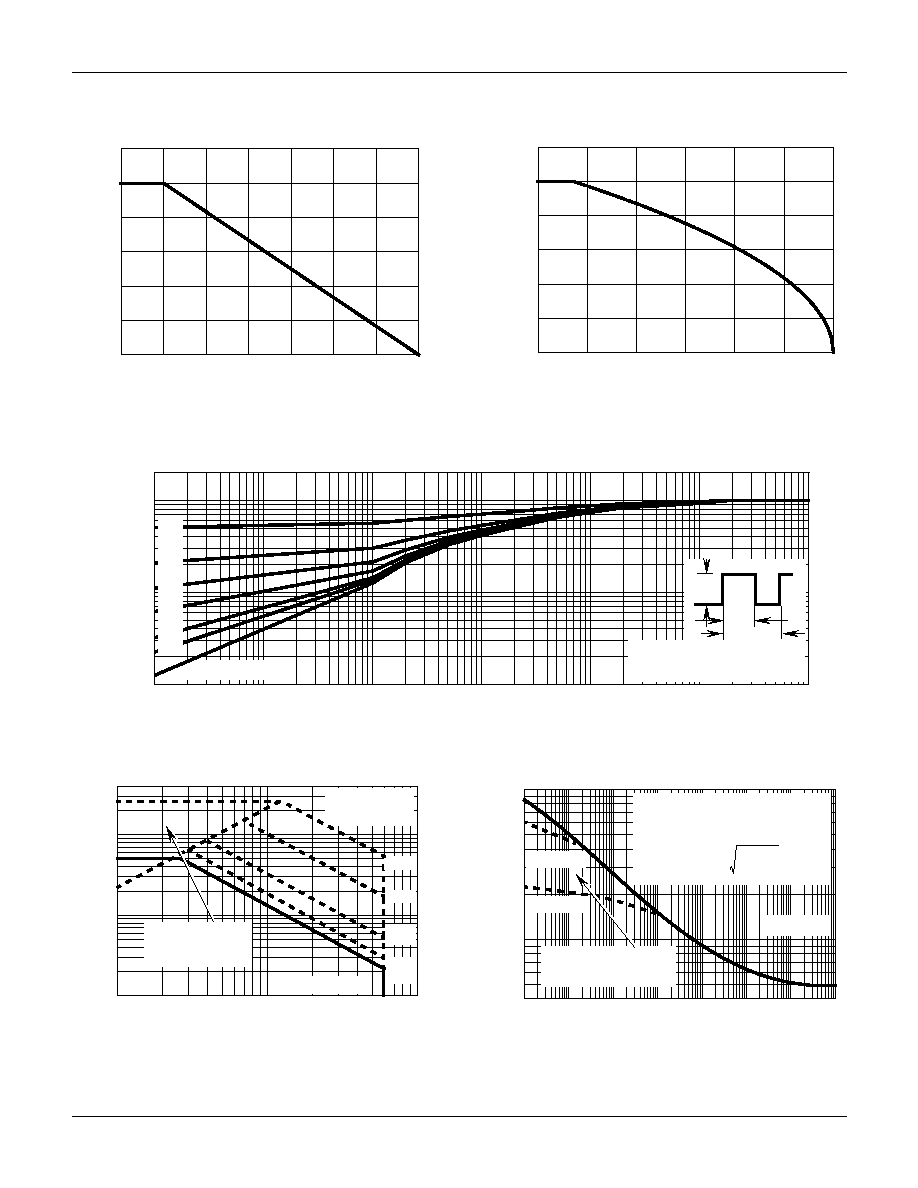
Typical Performance Curves
Unless Otherwise Specified
FIGURE 1. NORMALIZED POWER DISSIPATION vs CASE
TEMPERATURE
FIGURE 2. MAXIMUM CONTINUOUS DRAIN CURRENT vs
CASE TEMPERATURE
FIGURE 3. NORMALIZED MAXIMUM TRANSIENT THERMAL IMPEDANCE
FIGURE 4. FORWARD BIAS SAFE OPERATING AREA
FIGURE 5. PEAK CURRENT CAPABILITY
1.2
1.0
0.8
0.6
0.4
0.2
0
0
25
50
75
100
125
150
175
PO
WER DISSIP
A
TION MUL
TIPLIER
T
C
,
CASE TEMPERATURE (
o
C)
50
40
30
20
10
0
25
50
75
100
125
150
175
I
D
,
DRAIN CURRENT (A)
T
C
,
CASE TEMPERATURE (
o
C)
60
1
0.1
0.01
10
-5
10
-4
10
-3
10
-2
10
-1
10
0
10
1
t
1
, RECTANGULAR PULSE DURATION (s)
P
DM
NOTES:
DUTY FACTOR: D = t
1
/t
2
PEAK T
J
= P
DM
x Z
JC
x R
JC
+ T
C
SINGLE PULSE
t
1
t
2
THERMAL IMPED
ANCE
Z
JC
,
NORMALIZED
0.01
0.02
0.05
0.1
0.2
0.5
2
400
100
10
1
1
10
100
V
DS
,
DRAIN TO SOURCE VOLTAGE (V)
OPERATION IN THIS
AREA MAY BE
LIMITED BY r
DS(ON)
1ms
100
µs
10ms
100ms
DC
V
DSS(MAX)
= 60V
I
D
,
DRAIN CURRENT (A)
T
C
= 25
o
C
T
J
= MAX RATED
SINGLE PULSE
10
-3
10
-2
10
-1
10
0
10
1
10
2
10
3
10
4
10
2
10
3
t, PULSE WIDTH (ms)
V
GS
= 20V
V
GS
= 10V
TRANSCONDUCTANCE
MAY LIMIT CURRENT
IN THIS REGION
FOR TEMPERATURES ABOVE 25
o
C
DERATE PEAK CURRENT
CAPABILITY AS FOLLOWS:
I
I
25
175
T
C
≠
150
------------------------
=
I
DM
,
PEAK CURRENT (A)
40
T
C
= 25
o
C
RFG50N06, RFP50N06, RF1S50N06SM
©2002 Fairchild Semiconductor Corporation
RFG50N06, RFP50N06, RF1S50N06SM Rev. B
NOTE: Refer to Fairchild Application Notes 9321 and 9322.
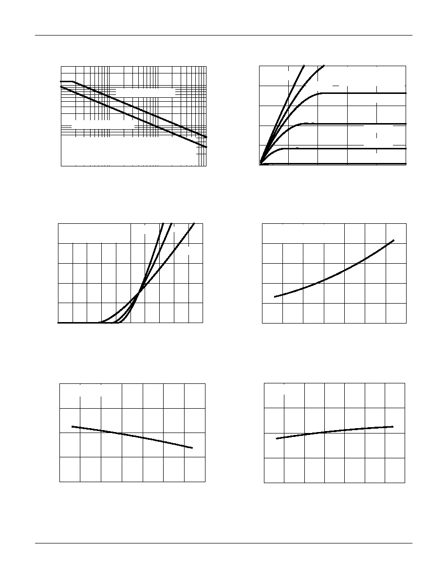
FIGURE 6. UNCLAMPED INDUCTIVE SWITCHING CAPABILITY
FIGURE 7. SATURATION CHARACTERISTICS
FIGURE 8. TRANSFER CHARACTERISTICS
FIGURE 9. NORMALIZED DRAIN TO SOURCE ON
RESISTANCE vs JUNCTION TEMPERATURE
FIGURE 10. NORMALIZED GATE THRESHOLD VOLTAGE vs
JUNCTION TEMPERATURE
FIGURE 11. NORMALIZED DRAIN TO SOURCE BREAKDOWN
VOLTAGE vs JUNCTION TEMPERATURE
Typical Performance Curves
Unless Otherwise Specified (Continued)
STARTING T
J
= 150
o
C
STARTING T
J
= 25
o
C
300
100
10
1
0.01
0.1
1
10
t
AV,
TIME IN AVALANCHE (ms)
If R = 0
t
AV
= (L) (I
AS
) / (1.3 RATED BV
DSS
- V
DD
)
If R
0
t
AV
= (L/R) ln [(I
AS
*R) / (1.3 RATED BV
DSS
- V
DD
) + 1]
I
AS
,
A
V
ALANCHE CURRENT (A)
125
100
75
50
25
0
0
1.5
3.0
4.5
6.0
7.5
I
D
,
DRAIN CURRENT (A)
V
DS
,
DRAIN TO SOURCE VOLTAGE (V)
V
GS
= 10V
V
GS
= 8V
V
GS
= 7V
V
GS
= 6V
V
GS
= 5V
V
GS
= 4V
PULSE DURATION = 80
µs
T
C
= 25
o
C
DUTY CYCLE = 0.5% MAX
0
1
2
3
4
5
6
7
8
9
10
V
GS
,
GATE TO SOURCE VOLTAGE (V)
I
D
,
DRAIN CURRENT (A)
125
100
75
50
25
0
PULSE DURATION = 80
µs
DUTY CYCLE = 0.5% MAX
-55
o
C
175
o
C
25
o
C
V
DD
= 15V
2.5
2.0
1.5
1.0
0.5
0
-80
-40
0
40
80
120
160
200
T
J
,
JUNCTION TEMPERATURE (
o
C)
NORMALIZED DRAIN
T
O
SOURCE
PULSE DURATION = 80
µs
V
GS
= 10V, I
D
= 50A
ON RESIST
ANCE
DUTY CYCLE = 0.5% MAX
2.0
1.5
1.0
0.5
0
-80
-40
0
40
80
160
120
200
THRESHOLD V
O
L
T
A
GE
T
J
,
JUNCTION TEMPERATURE (
o
C)
NORMALIZED GA
TE
V
GS
= V
DS
, I
D
= 250
µA
2.0
1.5
1.0
0.5
0
-80
-40
0
40
80
120
160
200
NORMALIZED DRAIN
T
O
SOURCE
BREAKDO
WN V
O
L
T
A
GE
T
J
,
JUNCTION TEMPERATURE (
o
C)
I
D
= 250
µA
RFG50N06, RFP50N06, RF1S50N06SM
©2002 Fairchild Semiconductor Corporation
RFG50N06, RFP50N06, RF1S50N06SM Rev. B
FIGURE 12. CAPACITANCE vs DRAIN TO SOURCE VOLTAGE
NOTE: Refer to Fairchild Application Notes AN7254 and AN7260.
FIGURE 13. NORMALIZED SWITCHING WAVEFORMS FOR
CONSTANT GATE CURRENT
Test Circuits and Waveforms
FIGURE 14. UNCLAMPED ENERGY TEST CIRCUIT
FIGURE 15. UNCLAMPED ENERGY WAVEFORMS
FIGURE 16. SWITCHING TIME TEST CIRCUIT
FIGURE 17. SWITCHING WAVEFORMS
Typical Performance Curves
Unless Otherwise Specified (Continued)
C
ISS
C
OSS
C
RSS
4000
3000
2000
1000
0
0
5
10
15
20
25
C
,
CAP
A
CIT
ANCE (pF)
V
DS
,
DRAIN TO SOURCE VOLTAGE
(V)
V
GS
= 0V, f = 1MHz
C
ISS
= C
GS
+ C
GD
C
RSS
= C
GD
C
OSS
= C
DS
+ C
GD
60
45
30
15
0
10
7.5
5.0
2.5
0
20
I
g(REF)
I
g(ACT)
80
I
g(REF)
I
g(ACT)
t, TIME (
µs)
V
DD
= BV
DSS
V
DD
= BV
DSS
0.75 BV
DSS
0.50 BV
DSS
0.25 BV
DSS
0.75 BV
DSS
0.50 BV
DSS
0.25 BV
DSS
V
DS
,
DRAIN
T
O
SOURCE
V
O
L
T
A
GE (V)
V
GS
,
GA
TE
T
O
SOURCE
V
O
L
T
A
GE (V)
R
L
= 1.2
I
g(REF)
= 1.45mA
V
GS
= 10V
t
P
V
GS
0.01
L
I
AS
+
-
V
DS
V
DD
R
G
DUT
VARY t
P
TO OBTAIN
REQUIRED PEAK I
AS
0V
V
DD
V
DS
BV
DSS
t
P
I
AS
t
AV
0
V
GS
R
L
R
GS
DUT
+
-
V
DD
V
DS
V
GS
t
ON
t
d(ON)
t
r
90%
10%
V
DS
90%
10%
t
f
t
d(OFF)
t
OFF
90%
50%
50%
10%
PULSE WIDTH
V
GS
0
0
RFG50N06, RFP50N06, RF1S50N06SM
©2002 Fairchild Semiconductor Corporation
RFG50N06, RFP50N06, RF1S50N06SM Rev. B
FIGURE 18. GATE CHARGE TEST CIRCUIT
FIGURE 19. GATE CHARGE WAVEFORMS
Test Circuits and Waveforms
(Continued)
R
L
V
GS
+
-
V
DS
V
DD
DUT
I
g(REF)
V
DD
Q
g(TH)
V
GS
= 2V
Q
g(10)
V
GS
= 10V
Q
g(TOT)
V
GS
= 20V
V
DS
V
GS
I
g(REF)
0
0
RFG50N06, RFP50N06, RF1S50N06SM
©2002 Fairchild Semiconductor Corporation
RFG50N06, RFP50N06, RF1S50N06SM Rev. B
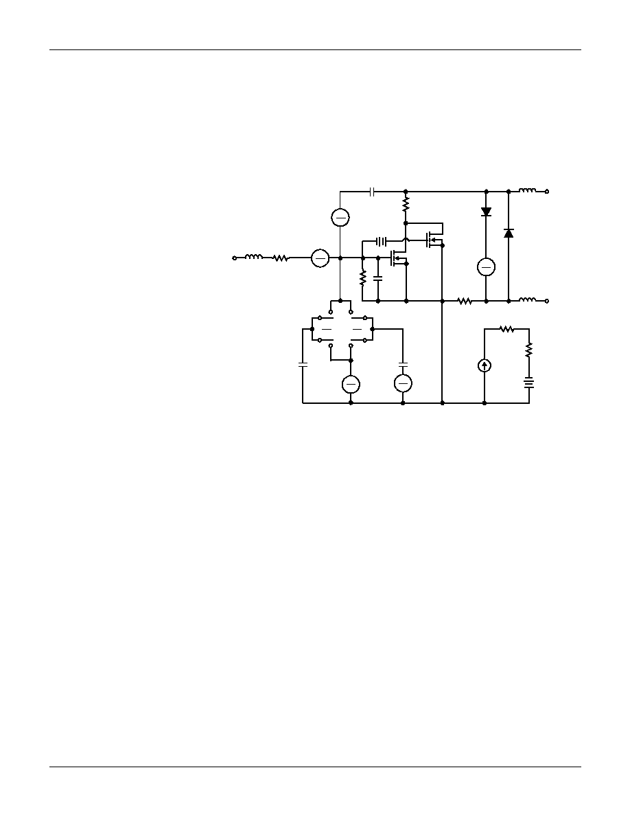
PSPICE Electrical Model
.SUBCKT RFP50N06 2 1 3
REV 2/22/93
*
NOM TEMP = 25
o
C
CA 12 8 3.68e-9
CB 15 14 3.625e-9
CIN 6 8 1.98e-9
DBODY 7 5 DBDMOD
DBREAK 5 11DBKMOD
DPLCAP 10 5 DPLCAPMOD
EBREAK 11 7 17 18 64.59
EDS 14 8 5 8 1
EGS 13 8 6 8 1
ESG 6 10 6 8 1
EVTO 20 6 18 8 1
IT 8 17 1
LDRAIN 2 5 1e-9
LGATE 1 9 5.65e-9
LSOURCE 3 7 4.13e-9
MOS1 16 6 8 8 MOSMOD M=0.99
MOS2 16 21 8 8 MOSMOD M=0.01
RBREAK 17 18 RBKMOD 1
RDRAIN 5 16 RDSMOD 1e-4
RGATE 9 20 0.690
RIN 6 8 1e9
RSOURCE 8 7 RDSMOD 12e-3
RVTO 18 19 RVTOMOD 1
S1A 6 12 13 8 S1AMOD
S1B 13 12 13 8 S1BMOD
S2A 6 15 14 13 S2AMOD
S2B 13 15 14 13 S2BMOD
VBAT 8 19 DC 1
VTO 21 6 0.678
.MODEL DBDMOD D (IS=9.85e-13 RS=4.91e-3 TRS1=2.07e-3 TRS2=2.51e-7 CJO=2.05e-9 TT=4.33e-8)
.MODEL DBKMOD D (RS=1.98e-1 TRS1=2.35E-4 TRS2=-3.83e-6)
.MODEL DPLCAPMOD D (CJO=1.42e-9 IS=1e-30 N=10)
.MODEL MOSMOD NMOS (VTO=3.65 KP=35 IS=1e-30 N=10 TOX=1 L=1u W=1u)
.MODEL RBKMOD RES (TC1=1.23e-3 TC2=-2.34e-7)
.MODEL RDSMOD RES (TC1=5.01e-3 TC2=1.49e-5)
.MODEL RVTOMOD RES (TC1=-5.03e-3 TC2=-5.16e-6)
.MODEL S1AMOD VSWITCH (RON=1e-5 ROFF=0.1 VON=-6.75 VOFF=-2.5)
.MODEL S1BMOD VSWITCH (RON=1e-5 ROFF=0.1 VON=-2.5 VOFF=-6.75)
.MODEL S2AMOD VSWITCH (RON=1e-5 ROFF=0.1 VON=-2.7 VOFF=2.3)
.MODEL S2BMOD VSWITCH (RON=1e-5 ROFF=0.1 VON=2.3 VOFF=-2.7)
.ENDS
NOTE: For further discussion of the PSPICE model consult A New PSPICE Sub-Circuit for the Power MOSFET Featuring Global Temperature
Options; authors, William J. Hepp and C. Frank Wheatley.
10
DPLCAP
RDRAIN
DBREAK
LDRAIN
DRAIN
SOURCE
LSOURCE
DBODY
RBREAK
RVTO
VBAT
+
-
19
IT
RSOURCE
EBREAK
MOS2
EDS
EGS
RIN
CIN
VTO
ESG
S1A
S2A
S2B
S1B
CB
CA
EVTO
RGATE
GATE
LGATE
5
2
18
17
7
11
21
8
6
16
20
9
1
12
15
14
13
13
8
14
13
+
-
+
-
+
-
+
-
+
-
+
-
MOS1
3
6
8
5
8
18
8
6
8
17
18
RFG50N06, RFP50N06, RF1S50N06SM

DISCLAIMER
FAIRCHILD SEMICONDUCTOR RESERVES THE RIGHT TO MAKE CHANGES WITHOUT FURTHER
NOTICE TO ANY PRODUCTS HEREIN TO IMPROVE RELIABILITY, FUNCTION OR DESIGN. FAIRCHILD
DOES NOT ASSUME ANY LIABILITY ARISING OUT OF THE APPLICATION OR USE OF ANY PRODUCT
OR CIRCUIT DESCRIBED HEREIN; NEITHER DOES IT CONVEY ANY LICENSE UNDER ITS PATENT
RIGHTS, NOR THE RIGHTS OF OTHERS.
TRADEMARKS
The following are registered and unregistered trademarks Fairchild Semiconductor owns or is authorized to use and is
not intended to be an exhaustive list of all such trademarks.
LIFE SUPPORT POLICY
FAIRCHILD'S PRODUCTS ARE NOT AUTHORIZED FOR USE AS CRITICAL COMPONENTS IN LIFE SUPPORT
DEVICES OR SYSTEMS WITHOUT THE EXPRESS WRITTEN APPROVAL OF FAIRCHILD SEMICONDUCTOR CORPORATION.
As used herein:
1. Life support devices or systems are devices or
systems which, (a) are intended for surgical implant into
the body, or (b) support or sustain life, or (c) whose
failure to perform when properly used in accordance
with instructions for use provided in the labeling, can be
reasonably expected to result in significant injury to the
user.
2. A critical component is any component of a life
support device or system whose failure to perform can
be reasonably expected to cause the failure of the life
support device or system, or to affect its safety or
effectiveness.
PRODUCT STATUS DEFINITIONS
Definition of Terms
Datasheet Identification
Product Status
Definition
Advance Information
Preliminary
No Identification Needed
Obsolete
This datasheet contains the design specifications for
product development. Specifications may change in
any manner without notice.
This datasheet contains preliminary data, and
supplementary data will be published at a later date.
Fairchild Semiconductor reserves the right to make
changes at any time without notice in order to improve
design.
This datasheet contains final specifications. Fairchild
Semiconductor reserves the right to make changes at
any time without notice in order to improve design.
This datasheet contains specifications on a product
that has been discontinued by Fairchild semiconductor.
The datasheet is printed for reference information only.
Formative or
In Design
First Production
Full Production
Not In Production
OPTOLOGICTM
OPTOPLANARTM
PACMANTM
POPTM
Power247TM
PowerTrench
QFETTM
QSTM
QT OptoelectronicsTM
Quiet SeriesTM
SILENT SWITCHER
FAST
FASTrTM
FRFETTM
GlobalOptoisolatorTM
GTOTM
HiSeCTM
ISOPLANARTM
LittleFETTM
MicroFETTM
MicroPakTM
MICROWIRETM
Rev. H4
Æ
ACExTM
BottomlessTM
CoolFETTM
CROSSVOLTTM
DenseTrenchTM
DOMETM
EcoSPARKTM
E
2
CMOS
TM
EnSigna
TM
FACTTM
FACT Quiet SeriesTM
SMART STARTTM
STAR*POWERTM
StealthTM
SuperSOTTM-3
SuperSOTTM-6
SuperSOTTM-8
SyncFETTM
TinyLogicTM
TruTranslationTM
UHCTM
UltraFET
Æ
Æ
Æ
STAR*POWER is used under license
VCXTM