 | ÐлекÑÑоннÑй компоненÑ: SGF15N90D | СкаÑаÑÑ:  PDF PDF  ZIP ZIP |
Äîêóìåíòàöèÿ è îïèñàíèÿ www.docs.chipfind.ru
©2002 Fairchild Semiconductor Corporation
SGF15N90D Rev. A1
IGBT
S
G
F15N90D
SGF15N90D
General Description
Insulated Gate Bipolar Transistors (IGBTs) with a trench
gate structure provide superior conduction and switching
performance in comparison with transistors having a planar
gate structure. They also have wide noise immunity. These
devices are very suitable for induction heating applications.
Features
· High speed switching
· Low saturation voltage : V
CE(sat)
= 2.0 V @ I
C
= 15A
· High input impedance
· Built-in fast recovery diode
Absolute Maximum Ratings
T
C
= 25
°
C unless otherwise noted
Notes :
(1) Repetitive rating : Pulse width limited by max. junction temperature
Thermal Characteristics
Symbol
Description
SGF15N90D
Units
V
CES
Collector-Emitter Voltage
900
V
V
GES
Gate-Emitter Voltage
±
25
V
I
C
Collector Current
@ T
C
= 25
°
C
15
A
Collector Current
@ T
C
= 100
°
C
12
A
I
CM (1)
Pulsed Collector Current
30
A
I
F
Diode Continuous Forward Current
@ T
C
= 100
°
C
12
A
P
D
Maximum Power Dissipation @ T
C
= 25
°
C
83
W
Maximum Power Dissipation
@ T
C
= 100
°
C
33
W
T
J
Operating Junction Temperature
-55 to +150
°
C
T
stg
Storage Temperature Range
-55 to +150
°
C
T
L
Maximum Lead Temp. for soldering
purposes,1/8" from case for 5 seconds
300
°
C
Symbol
Parameter
Typ.
Max.
Units
R
JC
(IGBT)
Thermal Resistance, Junction-to-Case
--
1.5
°
C
/
W
R
JC
(DIODE)
Thermal Resistance, Junction-to-Case
--
2.86
°
C
/
W
R
JA
Thermal Resistance, Junction-to-Ambient
--
40
°
C
/
W
Applications
Home appliances, induction heaters, induction hea 1 ting JARs, and microwave ovens.
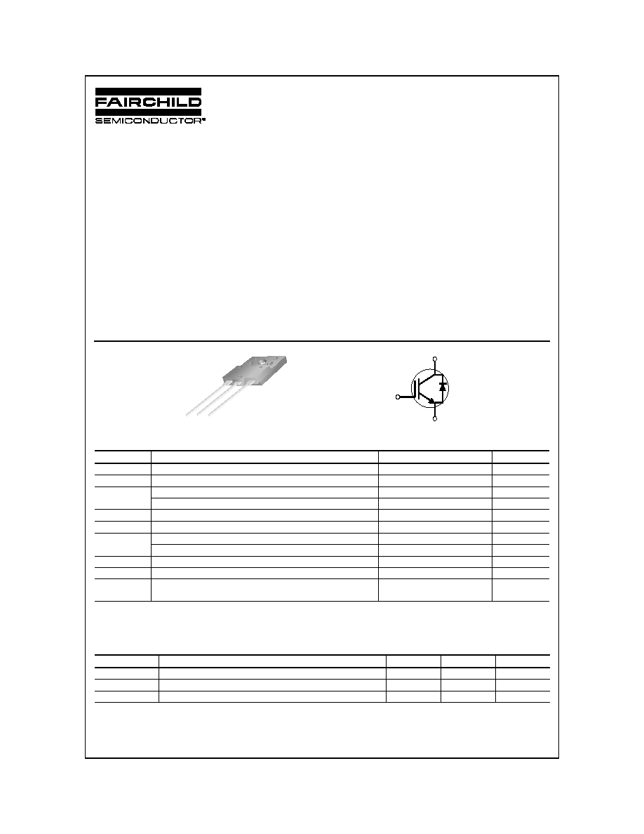
C
TO-3PF
G
C
E
G
C
E
SGF15N90D Rev. A1
S
G
F15N90D
©2002 Fairchild Semiconductor Corporation
Electrical Characteristics of the IGBT
T
C
= 25
°
C unless otherwise noted
Electrical Characteristics of DIODE
T
C
= 25
°
C unless otherwise noted
Symbol
Parameter
Test Conditions
Min.
Typ.
Max.
Units
Off Characteristics
BV
CES
Collector-Emitter Breakdown Voltage
V
GE
= 0V, I
C
= 250
µ
A
900
--
--
V
I
CES
Collector Cut-off Current
V
CE
= V
CES
, V
GE
= 0V
--
--
1.0
mA
I
GES
G-E Leakage Current
V
GE
= V
GES
, V
CE
= 0V
--
--
±
500
nA
On Characteristics
V
GE(th)
G-E Threshold Voltage
I
C
= 15mA, V
CE
= V
GE
4.0
5.0
7.0
V
V
CE(sat)
Collector to Emitter
Saturation Voltage
I
C
= 2.5A
,
V
GE
= 15V
--
1.4
1.8
V
I
C
= 15A
,
V
GE
= 15V
--
2.0
2.7
V
Dynamic Characteristics
C
ies
Input Capacitance
V
CE
=10V
,
V
GE
= 0V,
f = 1MHz
--
1500
--
pF
C
oes
Output Capacitance
--
80
--
pF
C
res
Reverse Transfer Capacitance
--
50
--
pF
Switching Characteristics
t
d(on)
Turn-On Delay Time
V
CC
= 600 V, I
C
= 15A,
R
G
= 51
, V
GE
= 15V,
Resistive Load, T
C
25
°
C
--
50
80
ns
t
r
Rise Time
--
180
280
ns
t
d(off)
Turn-Off Delay Time
--
150
230
ns
t
f
Fall Time
--
200
320
ns
Q
g
Total Gate Charge
V
CE
= 600 V, I
C
= 15A,
V
GE
= 15V
--
60
80
nC
Q
ge
Gate-Emitter Charge
--
15
--
nC
Q
gc
Gate-Collector Charge
--
20
--
nC
Symbol
Parameter
Test Conditions
Min.
Typ.
Max.
Units
V
FM
Diode Forward Voltage
I
F
= 4A
--
1.1
1.6
V
I
F
= 15A
--
1.45
1.7
V
t
rr
Diode Reverse Recovery Time
I
F
= 15A, di/dt = 20 A/
µ
s
--
0.8
1.2
us
I
R
Instantaneous Reverse Current
V
RRM
= 900V
--
0.03
1.2
uA
SGF15N90D Rev. A1
S
G
F15N90D
©2002 Fairchild Semiconductor Corporation
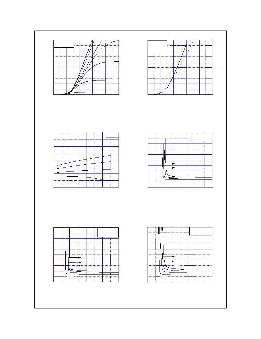
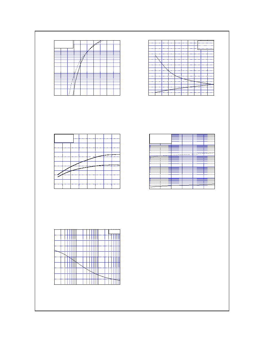
Fig 1. Typical Output Characteristics
Fig 2. Typical Saturation Voltage Characteristics
Fig 3. Saturation Voltage vs. Case
Temperature at Variant Current Level
Fig 4. Saturation Voltage vs. V
GE
Fig 5. Saturation Voltage vs. V
GE
Fig 6. Saturation Voltage vs. V
GE
0
1
2
3
4
5
0
10
20
30
40
50
Common Emitter
T
C
= 25
20V
15V
10V
9V
8V
7V
V
GE
= 6V
Co
l
l
e
ct
o
r
Cu
r
r
e
n
t
,
I
C
[A
]
Collector-Emitter Voltage, V
CE
[V]
0
1
2
3
4
5
0
10
20
30
40
50
Common Emitter
V
GE
= 15V
T
C
= 25
T
C
= 125
------
Collector Cu
rren
t, I
C
[A]
Collector-Emitter Voltage,V
CE
[V]
-50
0
50
100
150
1.0
1.5
2.0
2.5
3.0
V
GE
= 15V
15A
10A
I
C
= 5A
20A
C
o
llec
t
or-E
m
i
tte
r Vol
t
ag
e
, V
CE
[V
]
Case Temperature, T
C
[
]
4
8
12
16
20
0
2
4
6
8
10
15A
10A
20A
I
C
= 5A
Common Emitter
T
C
= -40
Collector-Em
i
tter Voltag
e, V
CE
[V]
Gate-Emitter Voltage, V
GE
[V]
4
8
12
16
20
0
2
4
6
8
10
20A
15A
10A
I
C
= 5A
Common Emitter
T
C
= 25
Co
llector
-Em
i
tt
er Vo
ltag
e,
V
CE
[V
]
Gate-Emitter Voltage, V
GE
[V]
4
8
12
16
20
0
2
4
6
8
10
20A
15A
10A
I
C
= 5A
Common Emitter
T
C
= 125
Collector-Em
i
tter Voltag
e, V
CE
[V]
Gate-Emitter Voltage, V
GE
[V]
SGF15N90D Rev. A1
S
G
F15N90D
©2002 Fairchild Semiconductor Corporation
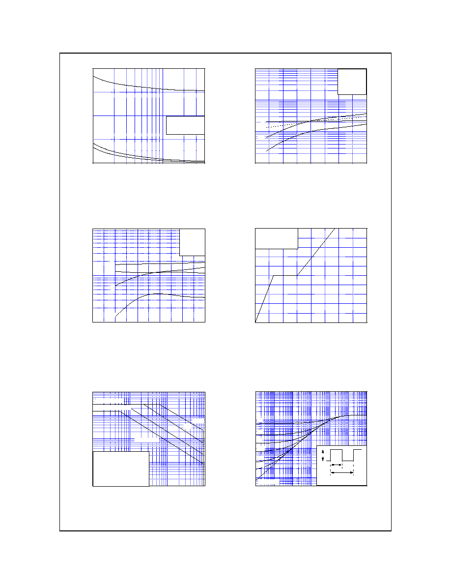
Fig 7. Capacitance Characteristics
Fig 8. Switching Characteristics vs.
Gate Resistance
Fig 9. Switching Characteristics vs.
Collector current
Fig 10. Gate Charge Characteristics
Fig 11. SOA Characteristics
1
10
1000
2000
Cres
Coes
Cies
Common Emitter
V
GE
= 0V, f = 1MHz
T
C
= 25
Ca
p
a
citan
c
e
[p
F]
Collector-Emitter Voltage, V
CE
[V]
0
50
100
150
200
10
100
1000
10000
V
CC
= 600V
I
C
= 15A
V
GE
=
±
15V
T
C
= 25
Ton
Toff
Tr
Tf
Sw
itch
in
g
T
i
m
e
[n
s]
Gate Resistance, R
G
[
]
0
20
40
60
80
0
3
6
9
12
15
Common Emitter
V
CC
= 600V, R
L
= 40
T
C
= 25
G
a
te-Em
i
tte
r Voltag
e, V
GE
[V]
Gate Charge, Q
g
[nC]
1
10
100
1000
0.01
0.1
1
10
100
Single Nonrepetitive Pulse
T
C
= 25
Curve must be darated
linearly with increase
in temperature
100us
1ms
10ms
DC Operation
I
C
MAX. (Pulsed)
I
C
MAX. (Continuous)
Coll
ecto
r Cu
r
r
en
t
,I
C
[A]
Collector-Emitter Voltage, V
CE
[V]
10
-5
10
-4
10
-3
10
-2
10
-1
10
0
10
1
0.01
0.1
1
10
0.5
0.2
0.1
0.05
0.02
0.01
single pulse
T
h
er
m
a
l
Re
sp
on
s
e
,
Zt
h
j
c
[
o
C/
W
]
Rectangular Pulse Duration [sec]
Fig 12. Transient Thermal Impedance of IGBT
Pdm
t1
t2
Duty factor D = t1 / t2
Peak Tj = Pdm
×
Zthjc + T
C
0
3
6
9
12
15
10
100
1000
Tf
Tdoff
Tr
Tdon
V
CC
=600V
R
G
=51
V
GE
=
±
15V
T
C
=25
S
witchin
g T
i
me
[ns]
Collector Current,Ic [A]
SGF15N90D Rev. A1
S
G
F15N90D
©2002 Fairchild Semiconductor Corporation
0
40
80
120
160
200
0.0
0.1
0.2
0.3
0.4
0.5
0.6
0.7
0.8
0.9
1.0
I
rr
t
rr
I
F
= 15A
T
C
= 25
di/dt [A/us]
R
e
v
e
rse
R
e
co
v
e
r
y
Ti
me
,
t
rr
[u
s]
0
10
20
30
40
50
60
70
80
90
100
Rever
s
e Rec
o
ver
y
Cu
r
r
e
n
t
,
I
rr
[A
]
Fig 14. Reverse Recovery Characteristics vs. di/dt
Fig 13. Forward Characteristics
Fig 15. Reverse Recovery Characteristics
vs. Forward current
Fig 16. Reverse Current vs. Reverse Voltage
Fig 17. Junction Capacitance
0.1
1
10
30
0.0
0.5
1.0
1.5
2.0
2.5
T
C
= 25
T
C
= 100
------
Forward Voltage, V
FM
[V]
F
o
rward C
u
rre
n
t, I
F
[A
]
0
5
10
15
20
0.0
0.2
0.4
0.6
0.8
1.0
1.2
I
rr
t
rr
di/dt = 20A/us
T
C
= 25
Forward Current, I
F
[A]
Re
ve
r
s
e
Re
c
o
ve
r
y
T
i
m
e
,
t
rr
[u
s
]
0
2
4
6
8
10
12
Re
ve
r
s
e
Re
c
o
ve
r
y
Cu
r
r
e
n
t
,
I
rr
[A
]
0
300
600
900
0.01
0.1
1
10
100
1000
T
C
= 25
T
C
= 150
------
Rev
e
rse Cu
rren
t, I
R
[u
A]
Reverse Voltage, V
R
[V]
0.1
1
10
100
0
20
40
60
80
100
T
C
= 25
J
u
n
c
ti
on
Ca
p
a
cita
n
ce,
C
j
[p
F
]
Reverse Voltage, V
R
[V]