 | ÐлекÑÑоннÑй компоненÑ: SGR6N60UF | СкаÑаÑÑ:  PDF PDF  ZIP ZIP |
Äîêóìåíòàöèÿ è îïèñàíèÿ www.docs.chipfind.ru
©2002 Fairchild Semiconductor Corporation
SGR6N60UF Rev. A1
IGBT
S
G
R6N60UF
SGR6N60UF
Ultra-Fast IGBT
General Description
Fairchild's UF series of Insulated Gate Bipolar Transistors
(IGBTs) provides low conduction and switching losses.
The UF series is designed for applications such as motor
control and general inverters where high speed switching is
a required feature.
Features
· High speed switching
· Low saturation voltage : V
CE(sat)
= 2.1 V @ I
C
= 3A
· High input impedance
Absolute Maximum Ratings
T
C
= 25
°
C unless otherwise noted
Notes :
(1) Repetitive rating : Pulse width limited by max. junction temperature
Thermal Characteristics
Notes :
(2) Mounted on 1" squre PCB (FR4 or G-10 Material)
Symbol
Description
SGR6N60UF
Units
V
CES
Collector-Emitter Voltage
600
V
V
GES
Gate-Emitter Voltage
±
20
V
I
C
Collector Current
@ T
C
= 25
°
C
6
A
Collector Current
@ T
C
= 100
°
C
3
A
I
CM (1)
Pulsed Collector Current
25
A
P
D
Maximum Power Dissipation
@ T
C
= 25
°
C
30
W
Maximum Power Dissipation
@ T
C
= 100
°
C
12
W
T
J
Operating Junction Temperature
-55 to +150
°
C
T
stg
Storage Temperature Range
-55 to +150
°
C
T
L
Maximum Lead Temp. for Soldering
Purposes, 1/8" from Case for 5 Seconds
300
°
C
Symbol
Parameter
Typ.
Max.
Units
R
JC
Thermal Resistance, Junction-to-Case
--
4.0
°
C
/
W
R
JA
Thermal Resistance, Junction-to-Ambient (PCB Mount)
(2)
--
50
°
C
/
W
Applications
AC & DC motor controls, general purpose inverters, robotics, and servo controls.
G
C
E
G
C
E
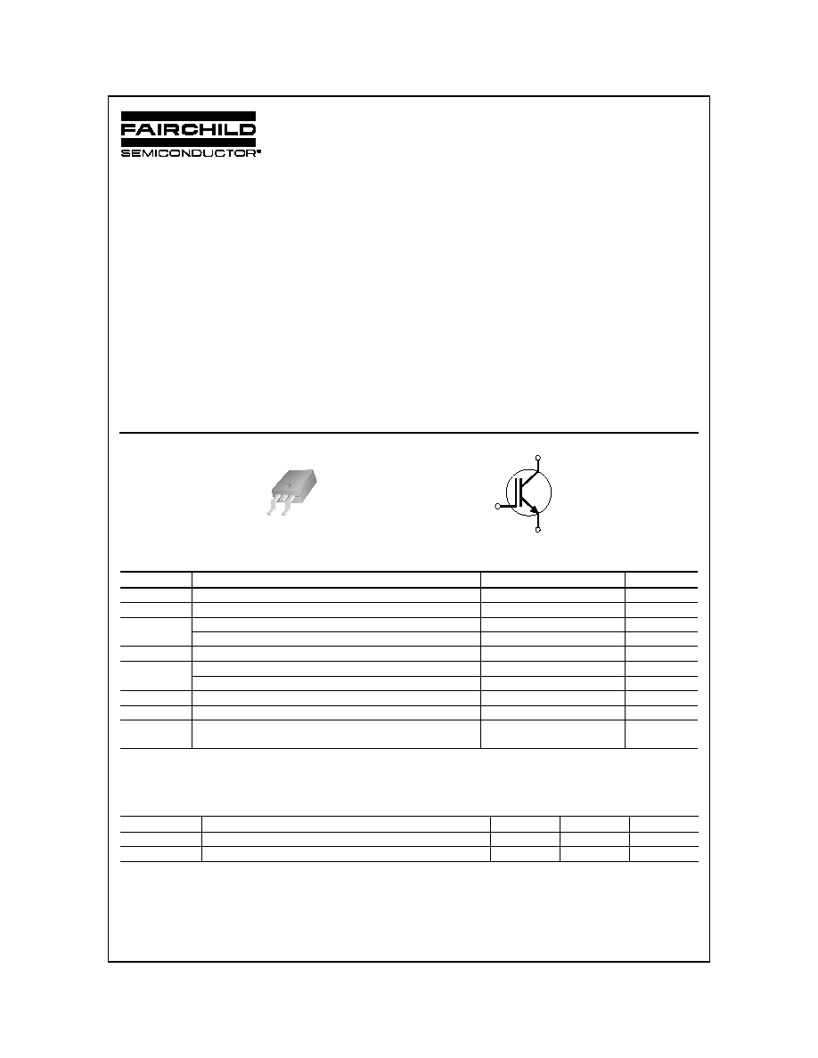
D-PAK
G E
C
SGR6N60UF Rev. A1
S
G
R6N60UF
©2002 Fairchild Semiconductor Corporation
Electrical Characteristics of the IGBT
T
C
= 25
°
C unless otherwise noted
Symbol
Parameter
Test Conditions
Min.
Typ.
Max.
Units
Off Characteristics
BV
CES
Collector-Emitter Breakdown Voltage
V
GE
= 0V, I
C
= 250uA
600
--
--
V
B
VCES
/
T
J
Temperature Coefficient of Breakdown
Voltage
V
GE
= 0V, I
C
= 1mA
--
0.6
--
V/
°
C
I
CES
Collector Cut-Off Current
V
CE
= V
CES
, V
GE
= 0V
--
--
250
uA
I
GES
G-E Leakage Current
V
GE
= V
GES
, V
CE
= 0V
--
--
± 100
nA
On Characteristics
V
GE(th)
G-E Threshold Voltage
I
C
= 3mA, V
CE
= V
GE
3.5
4.5
6.5
V
V
CE(sat)
Collector to Emitter
Saturation Voltage
I
C
= 3A
,
V
GE
= 15V
--
2.1
2.6
V
I
C
= 6A
,
V
GE
= 15V
--
2.6
--
V
Dynamic Characteristics
C
ies
Input Capacitance
V
CE
= 30V
,
V
GE
= 0V,
f = 1MHz
--
220
--
pF
C
oes
Output Capacitance
--
22
--
pF
C
res
Reverse Transfer Capacitance
--
7
--
pF
Switching Characteristics
t
d(on)
Turn-On Delay Time
V
CC
= 300 V, I
C
= 3A,
R
G
= 80
, V
GE
= 15V,
Inductive Load, T
C
= 25
°
C
--
15
--
ns
t
r
Rise Time
--
25
--
ns
t
d(off)
Turn-Off Delay Time
--
60
130
ns
t
f
Fall Time
--
70
150
ns
E
on
Turn-On Switching Loss
--
57
--
uJ
E
off
Turn-Off Switching Loss
--
25
--
uJ
E
ts
Total
Switching
Loss
--
82
120
uJ
t
d(on)
Turn-On Delay Time
V
CC
= 300 V, I
C
= 3A,
R
G
= 80
, V
GE
= 15V
,
Inductive Load, T
C
= 125
°
C
--
22
--
ns
t
r
Rise Time
--
32
--
ns
t
d(off)
Turn-Off Delay Time
--
80
200
ns
t
f
Fall Time
--
122
300
ns
E
on
Turn
-
On Switching Loss
--
65
--
uJ
E
off
Turn
-
Off Switching Loss
--
46
--
uJ
E
ts
Total
Switching
Loss
--
111
170
uJ
Q
g
Total Gate Charge
V
CE
= 300 V, I
C
= 3A,
V
GE
= 15V
--
15
22
nC
Q
ge
Gate-Emitter Charge
--
5
8
nC
Q
gc
Gate-Collector Charge
--
4
6
nC
L
e
Internal Emitter Inductance
Measured 5mm from PKG
--
7.5
--
nH
SGR6N60UF Rev. A1
S
G
R6N60UF
©2002 Fairchild Semiconductor Corporation
0
4
8
12
16
20
0
4
8
12
16
20
Common Emitter
T
C
= 125
6A
3A
I
C
= 1.5A
C
o
ll
ec
tor
- E
m
itte
r
V
o
lta
g
e
,
V
CE
[V
]
Gate - Emitter Voltage, V
GE
[V]
0
4
8
12
16
20
0
4
8
12
16
20
Common Emitter
T
C
= 25
6A
3A
I
C
= 1.5A
Col
l
ec
to
r - Em
i
t
t
e
r
V
o
l
t
ag
e,
V
CE
[V
]
Gate - Emitter Voltage, V
GE
[V]
0
2
4
6
8
0.1
1
10
100
1000
Duty cycle : 50%
T
C
= 100
Power Dissipation = 9W
V
CC
= 300V
Load Current : peak of square wave
Frequency [KHz]
Lo
ad
C
u
rre
n
t
[A
]
0
30
60
90
120
150
0
1
2
3
4
6A
3A
I
C
= 1.5A
Common Emitter
V
GE
= 15V
Col
l
e
ct
or
-
Em
i
t
t
e
r
Vol
t
age,
V
CE
[V
]
Case Temperature, T
C
[
]
0.5
1
10
0
3
6
9
12
15
Common Emitter
V
GE
= 15V
T
C
= 25
T
C
= 125
C
o
lle
cto
r
C
u
rre
n
t,
I
C
[A
]
Collector - Emitter Voltage, V
CE
[V]
0
2
4
6
8
0
5
10
15
20
25
30
20V
12V
15V
V
GE
= 10V
Common Emitter
T
C
= 25
Co
l
l
ect
o
r
Cu
r
r
e
n
t
,
I
C
[A
]
Collector - Emitter Voltage, V
CE
[V]
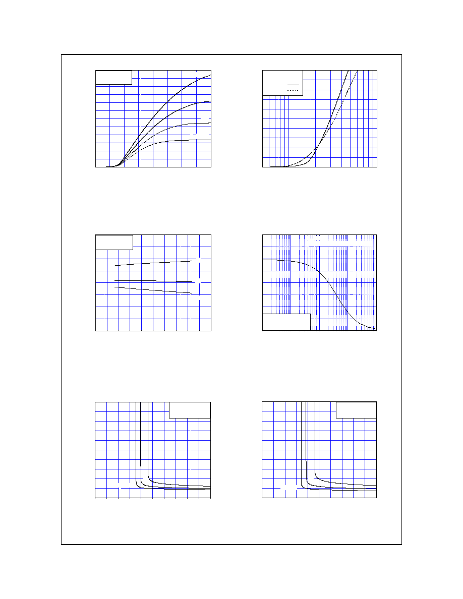
Fig 1. Typical Output Characteristics
Fig 2. Typical Saturation Voltage
Characteristics
Fig 3. Saturation Voltage vs. Case
Temperature at Variant Current Level
Fig 4. Load Current vs. Frequency
Fig 5. Saturation Voltage vs. V
GE
Fig 6. Saturation Voltage vs. V
GE
SGR6N60UF Rev. A1
S
G
R6N60UF
©2002 Fairchild Semiconductor Corporation
1
10
100
400
5
10
100
300
Eoff
Eon
Eoff
Common Emitter
V
CC
= 300V, V
GE
=
±
15V
I
C
= 3A
T
C
= 25
T
C
= 125
S
w
it
c
h
in
g
L
o
s
s
[u
J
]
Gate Resistance, R
G
[
]
1
10
100
400
10
100
Common Emitter
V
CC
= 300V, V
GE
=
±
15V
I
C
= 3A
T
C
= 25
T
C
= 125
Ton
Tr
S
w
it
c
h
in
g
T
i
m
e
[
n
s
]
Gate Resistance, R
G
[
]
1
10
100
400
50
100
600
Toff
Tf
Toff
Tf
Common Emitter
V
CC
= 300V, V
GE
=
±
15V
I
C
= 3A
T
C
= 25
T
C
= 125
S
w
it
c
h
in
g
T
i
m
e
[n
s
]
Gate Resistance, R
G
[
]
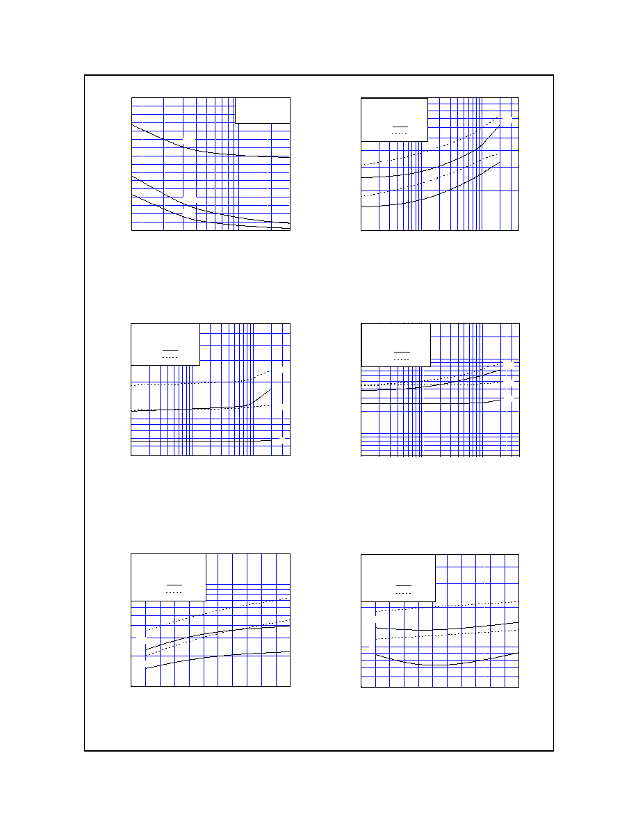
Fig 7. Capacitance Characteristics
Fig 8. Turn-On Characteristics vs.
Gate Resistance
Fig 9. Turn-Off Characteristics vs.
Gate Resistance
Fig 10. Switching Loss vs. Gate Resistance
Fig 11. Turn-On Characteristics vs.
Collector Current
Fig 12. Turn-Off Characteristics vs.
Collector Current
1
2
3
4
5
6
50
100
500
Toff
Tf
Common Emitter
V
CC
= 300V, V
GE
=
±
15V
R
G
= 80
T
C
= 25
T
C
= 125
Sw
i
t
ch
i
n
g
T
i
m
e
[n
s]
Collector Current, I
C
[A]
1
2
3
4
5
6
10
100
200
Ton
Tr
Common Emitter
V
CC
= 300V, V
GE
=
±
15V
R
G
= 80
T
C
= 25
T
C
= 125
Sw
i
t
ch
i
n
g T
i
m
e
[
n
s
]
Collector Current, I
C
[A]
1
10
30
0
50
100
150
200
250
300
350
400
Cres
Coes
Cies
Common Emitter
V
GE
= 0V, f = 1MHz
T
C
= 25
C
a
p
a
c
i
ta
n
c
e
[pF
]
Collector - Emitter Voltage, V
CE
[V]
SGR6N60UF Rev. A1
S
G
R6N60UF
©2002 Fairchild Semiconductor Corporation
10
-5
10
-4
10
-3
10
-2
10
-1
10
0
10
1
0.01
0.1
1
10
0.5
0.2
0.1
0.05
0.02
0.01
single pulse
T
h
erm
a
l
Resp
on
se, Zt
h
j
c [
/W
]
Rectangular Pulse Duration [sec]
1
10
100
1000
0.1
1
10
50
Safe Operating Area
V
GE
=20V, T
C
=100
o
C
C
o
lle
c
t
o
r
C
u
rre
n
t, I
C
[A
]
Collector-Emitter Voltage, V
CE
[V]
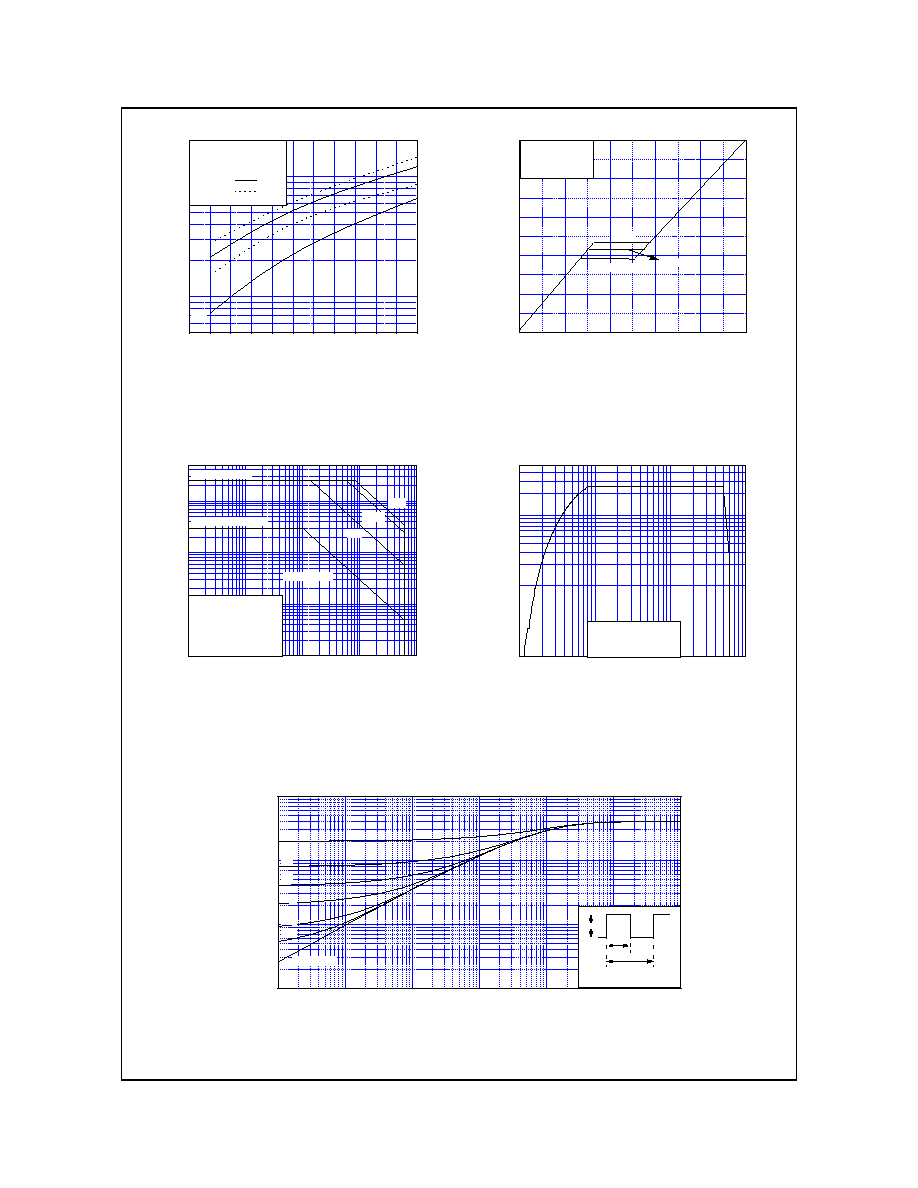
Fig 14. Gate Charge Characteristics
Fig 15. SOA Characteristics
Fig 16. Turn-Off SOA Characteristics
Fig 13. Switching Loss vs. Collector Current
Pdm
t1
t2
Duty factor D = t1 / t2
Peak Tj = Pdm
×
Zthjc + T
C
Fig 17. Transient Thermal Impedance of IGBT
0
3
6
9
12
15
0
3
6
9
12
15
300 V
200 V
V
CC
= 100 V
Common Emitter
R
L
= 100
Tc = 25
G
a
te
- E
m
itte
r V
o
lta
g
e
,
V
GE
[
V
]
Gate Charge, Q
g
[ nC ]
1
2
3
4
5
6
5
10
100
200
Eoff
Eon
Eon
Eoff
Common Emitter
V
CC
= 300V, V
GE
=
±
15V
R
G
= 80
T
C
= 25
T
C
= 125
Sw
i
t
ch
i
n
g Los
s [
u
J]
Collector Current, I
C
[A]
0.3
1
10
100
1000
0.01
0.1
1
10
50
Single Nonrepetitive
Pulse T
C
= 25
Curves must be derated
linearly with increase
in temperature
50us
100us
1
DC Operation
Ic MAX. (Continuous)
Ic MAX. (Pulsed)
C
o
l
l
ec
to
r C
u
r
r
en
t,
I
C
[A
]
Collector-Emitter Voltage, V
CE
[V]