 | ÐлекÑÑоннÑй компоненÑ: SI7463DP | СкаÑаÑÑ:  PDF PDF  ZIP ZIP |
Äîêóìåíòàöèÿ è îïèñàíèÿ www.docs.chipfind.ru
FEATURES
D TrenchFETr Power MOSFET
D New Low Thermal Resistance PowerPAKr
Package with Low 1.07-mm Profile
APPLICATIONS
D Automotive
- 12-V Boardnet
- High-Side Switches
- Motor Drives
Si7463DP
Vishay Siliconix
Document Number: 72440
S-32411--Rev. B, 24-Nov-03
www.vishay.com
1
P-Channel 40-V (D-S) MOSFET
PRODUCT SUMMARY
V
DS
(V)
r
DS(on)
(W)
I
D
(A)
-40
0.0092 @ V
GS
= -10 V
-18.6
-40
0.014 @ V
GS
= -4.5 V
-15
1
2
3
4
5
6
7
8
S
S
S
G
D
D
D
D
6.15 mm
5.15 mm
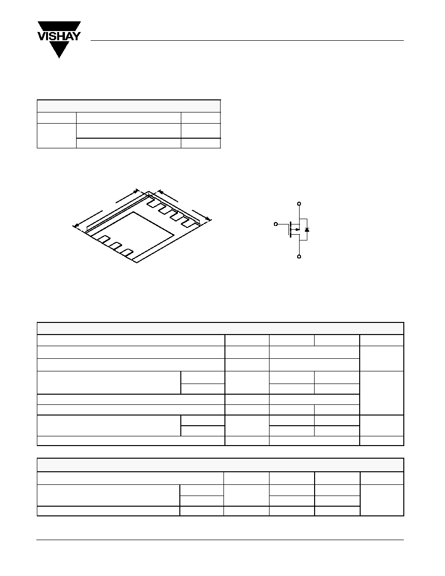
PowerPAK SO-8
Bottom View
S
G
D
P-Channel MOSFET
Ordering Information: Si7463DP-T1--E3
ABSOLUTE MAXIMUM RATINGS (T
A
= 25_C UNLESS OTHERWISE NOTED)
Parameter
Symbol
10 secs
Steady State
Unit
Drain-Source Voltage
V
DS
-40
V
Gate-Source Voltage
V
GS
"20
V
Continuous Drain Current
(T
J
= 150_C)
a
T
A
= 25_C
I
D
-18.6
-11
Continuous Drain Current
(T
J
= 150_C)
a
T
A
= 70_C
I
D
-15
-8.9
A
Pulsed Drain Current
I
DM
-60
A
continuous Source Current (Diode Conduction)
a
I
S
-4.5
-1.6
Maximum Power Dissipation
a
T
A
= 25_C
P
D
5.4
1.9
W
Maximum Power Dissipation
a
T
A
= 70_C
P
D
3.4
1.2
W
Operating Junction and Storage Temperature Range
T
J
, T
stg
-55 to 150
_C
THERMAL RESISTANCE RATINGS
Parameter
Symbol
Typical
Maximum
Unit
M i
J
ti
t A bi t
a
t v 10 sec
R
18
23
Maximum Junction-to-Ambient
a
Steady State
R
thJA
52
65
_C/W
Maximum Junction-to-Case (Drain)
Steady State
R
thJC
1.0
1.3
C/W
Notes
a.
Surface Mounted on 1" x 1" FR4 Board.
Si7463DP
Vishay Siliconix
www.vishay.com
2
Document Number: 72440
S-32411--Rev. B, 24-Nov-03
SPECIFICATIONS (T
J
= 25_C UNLESS OTHERWISE NOTED)
Parameter
Symbol
Test Condition
Min
Typ
Max
Unit
Static
Gate Threshold Voltage
V
GS(th)
V
DS
= V
GS
, I
D
= -250 mA
-1
-3
V
Gate-Body Leakage
I
GSS
V
DS
= 0 V, V
GS
= "20
V
"100
nA
Zero Gate Voltage Drain Current
I
DSS
V
DS
= -40 V, V
GS
= 0 V
-1
mA
Zero Gate Voltage Drain Current
I
DSS
V
DS
= -40 V, V
GS
= 0 V, T
J
= 70_C
-10
mA
On-State Drain Current
a
I
D(on)
V
DS
v -5 V, V
GS
= -10 V
-40
A
Drain Source On State Resistance
a
r
DS( )
V
GS
= -10 V, I
D
= -18.6 A
0.0075
0.0092
W
Drain-Source On-State Resistance
a
r
DS(on)
V
GS
= -4.5 V, I
D
= -15 A
0.011
0.014
W
Forward Transconductance
a
g
fs
V
DS
= -15
V, I
D
= -18.6 A
50
S
Diode Forward Voltage
a
V
SD
I
S
= -4.5 A, V
GS
= 0 V
-0.8
-1.2
V
Dynamic
b
Total Gate Charge
Q
g
121
140
Gate-Source Charge
Q
gs
V
DS
= -20 V,
V
GS
= -10 V, I
D
= -18.6 A
19.2
nC
Gate-Drain Charge
Q
gd
30.3
Gate-Resistance
R
g
2.7
W
Turn-On Delay Time
t
d(on)
20
30
Rise Time
t
r
V
DD
= -20 V, R
L
= 20 W
25
40
Turn-Off Delay Time
t
d(off)
V
DD
= -20 V, R
L
= 20 W
I
D
^ -1 A, V
GEN
= -10 V, R
G
= 6 W
200
300
ns
Fall Time
t
f
100
150
Source-Drain Reverse Recovery Time
t
rr
I
F
= -4.5 A, di/dt = 100 A/ms
45
70
Notes
a.
Pulse test; pulse width v 300 ms, duty cycle v 2%.
b.
Guaranteed by design, not subject to production testing.
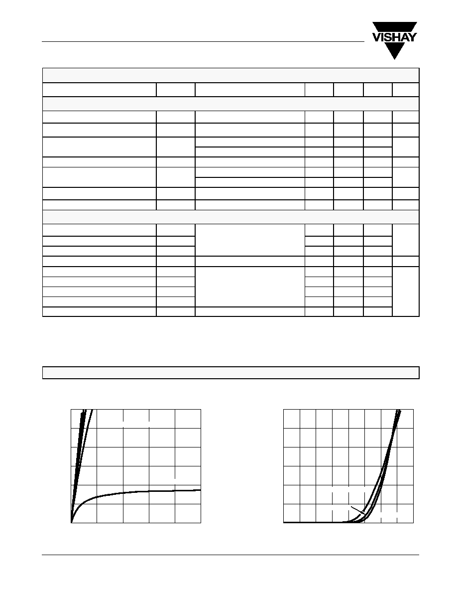
TYPICAL CHARACTERISTICS (25_C UNLESS NOTED)
0
10
20
30
40
50
60
0.0
0.5
1.0
1.5
2.0
2.5
3.0
3.5
4.0
0
10
20
30
40
50
60
0
1
2
3
4
5
V
GS
= 10 thru 4 V
25_C
T
C
= 125_C
-55_C
3 V
Output Characteristics
Transfer Characteristics
V
DS
- Drain-to-Source Voltage (V)
-
Drain Current (A)
I
D
V
GS
- Gate-to-Source Voltage (V)
-
Drain Current (A)
I
D
Si7463DP
Vishay Siliconix
Document Number: 72440
S-32411--Rev. B, 24-Nov-03
www.vishay.com
3
TYPICAL CHARACTERISTICS (25_C UNLESS NOTED)
V
SD
- Source-to-Drain Voltage (V)
0.00
0.01
0.02
0.03
0.04
0
2
4
6
8
10
-
On-Resistance (
r
DS(on)
W
)
V
GS
- Gate-to-Source Voltage (V)
0.0
0.2
0.4
0.6
0.8
1.0
1.2
0.000
0.002
0.004
0.006
0.008
0.010
0.012
0.014
0.016
0
10
20
30
40
50
60
0
2
4
6
8
10
0
25
50
75
100
125
0.6
0.8
1.0
1.2
1.4
1.6
-50
-25
0
25
50
75
100
125
150
0
1000
2000
3000
4000
5000
6000
7000
8000
0
8
16
24
32
40
C
rss
C
oss
C
iss
V
DS
= 15 V
I
D
= 18.6 A
V
GS
= 10 V
I
D
= 18.6 A
V
GS
= 10 V
Gate Charge
On-Resistance vs. Drain Current
-
Gate-to-Source V
oltage (V)
Q
g
- Total Gate Charge (nC)
V
DS
- Drain-to-Source Voltage (V)
C
-
Capacitance (pF)
V
GS
-
On-Resistance (
r
DS(on)
W
)
I
D
- Drain Current (A)
Capacitance
On-Resistance vs. Junction Temperature
T
J
- Junction Temperature (_C)
(Normalized)
-
On-Resistance (
r
DS(on)
W
)
T
J
= 150_C
T
J
= 25_C
I
D
= 18.6 A
100
10
1
Source-Drain Diode Forward Voltage
On-Resistance vs. Gate-to-Source Voltage
-
Source Current (A)
I
S
V
GS
= 4.5 V
I
D
= 5 A
Si7463DP
Vishay Siliconix
www.vishay.com
4
Document Number: 72440
S-32411--Rev. B, 24-Nov-03
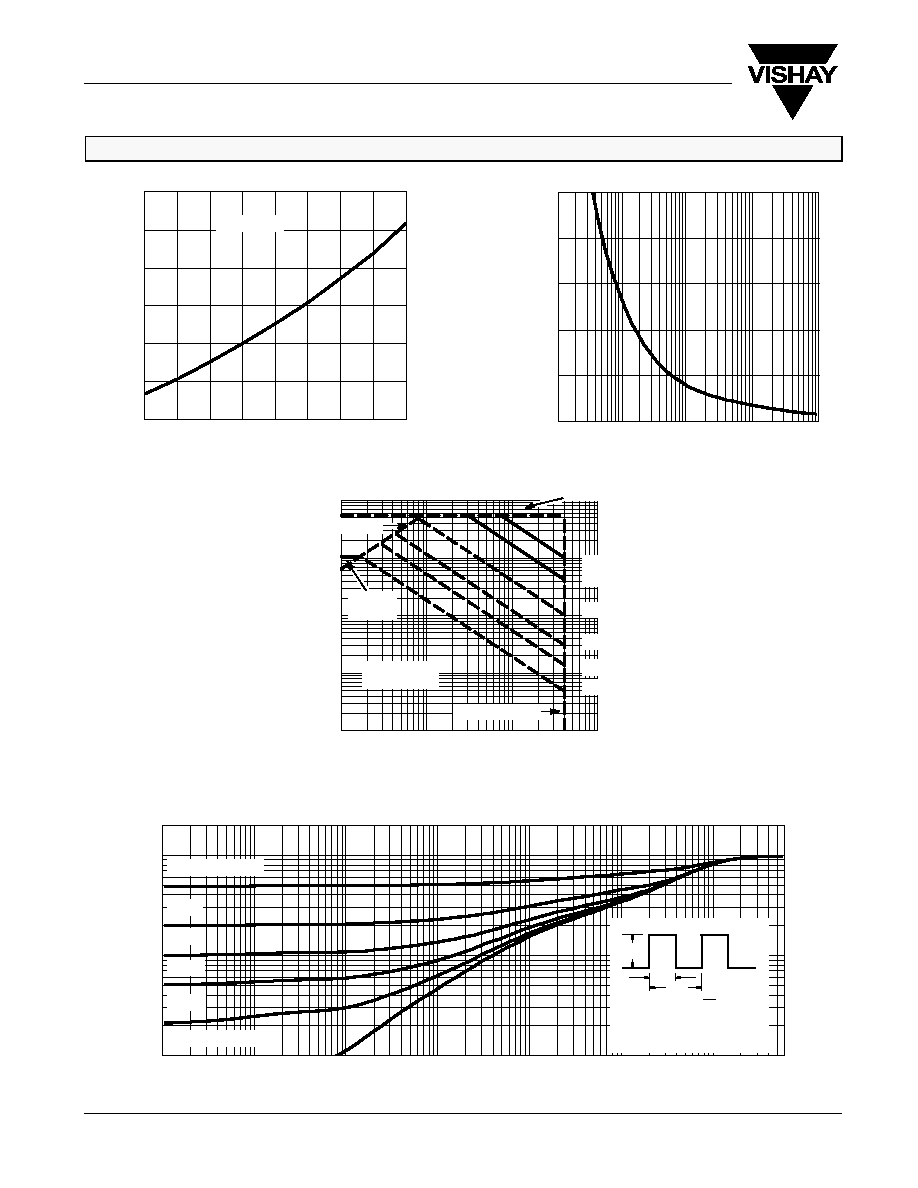
TYPICAL CHARACTERISTICS (25_C UNLESS NOTED)
10
-3
10
-2
1
10
600
10
-1
10
-4
100
0.01
0
10
80
100
20
100
0.1
Single Pulse Power, Juncion-To-Ambient
Time (sec)
60
40
Power (W)
2
1
0.1
0.01
0.2
0.1
0.05
0.02
Single Pulse
Duty Cycle = 0.5
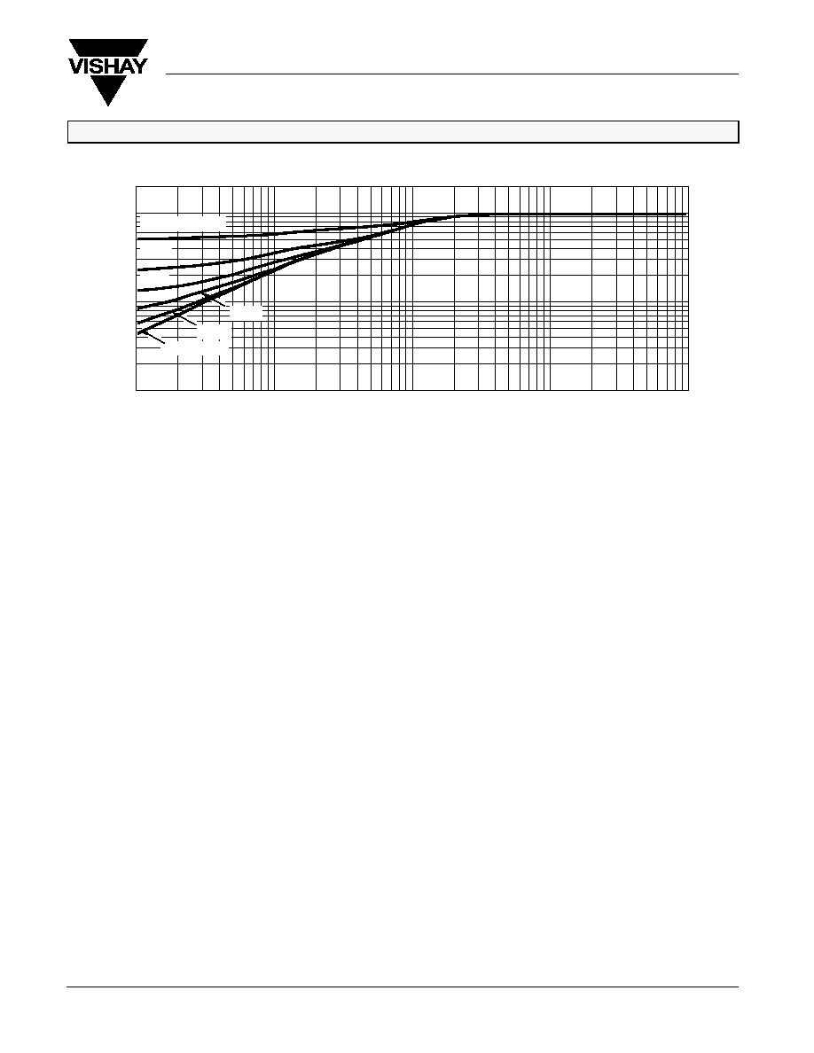
Normalized Thermal Transient Impedance, Junction-to-Ambient
Square Wave Pulse Duration (sec)
Normalized Ef
fective
T
ransient
Thermal Impedance
1. Duty Cycle, D =
2. Per Unit Base = R
thJA
= 52_C/W
3. T
JM
- T
A
= P
DM
Z
thJA(t)
t
1
t
2
t
1
t
2
Notes:
4. Surface Mounted
P
DM
1
-0.4
-0.2
0.0
0.2
0.4
0.6
0.8
-50
-25
0
25
50
75
100
125
150
I
D
= 250 mA
Threshold Voltage
V
ariance (V)
V
GS(th)
T
J
- Temperature (_C)
Safe Operating Area
V
DS
- Drain-to-Source Voltage (V)
100
1
0.1
1
10
100
0.01
10
T
A
= 25_C
Single Pulse
-
Drain Current (A)
I
D
P(t) = 10
dc
0.1
I
DM
Limited
I
D(on)
Limited
BV
DSS
Limited
P(t) = 1
P(t) = 0.1
P(t) = 0.01
P(t) = 0.001
r
DS(on)
Limited
Si7463DP
Vishay Siliconix
Document Number: 72440
S-32411--Rev. B, 24-Nov-03
www.vishay.com
5
TYPICAL CHARACTERISTICS (25_C UNLESS NOTED)
10
-3
10
-2
1
10
-1
10
-4
2
1
0.1
0.01
0.2
0.1
0.05
0.02
Single Pulse
Duty Cycle = 0.5
Normalized Thermal Transient Impedance, Junction-to-Case
Square Wave Pulse Duration (sec)
Normalized Ef
fective
T
ransient
Thermal Impedance