 | –≠–ª–µ–∫—Ç—Ä–æ–Ω–Ω—ã–π –∫–æ–º–ø–æ–Ω–µ–Ω—Ç: MPC5554 | –°–∫–∞—á–∞—Ç—å:  PDF PDF  ZIP ZIP |

© Freescale Semiconductor, Inc., 2005. All rights reserved.
Freescale Semiconductor
Product Brief
MPC5554PB
Rev. 2.1, 06/2005
Table of Contents
The MPC5554 is the first member of a family of next
generation microcontrollers based on the PowerPC
TM
Book E architecture that enhances the PowerPC
architecture's fit in embedded applications. It is 100%
user mode compatible (with floating point library) with
the classic PowerPC instruction set. This document
provides an overview of the MPC5554 microcontroller
features, including the major functional components.
The MPC5554 device's on-chip modules include the
following:
∑
Single issue, 32-bit PowerPC Book E-compliant
e200z6 CPU core complex
∑
64-channel enhanced direct memory access
controller (eDMA)
∑
Interrupt controller (INTC) capable of handling
286 selectable-priority interrupt sources
∑
Frequency modulated phase-locked loop
(FMPLL)
∑
External bus interface (EBI) with error
correction status module (ECSM)
∑
System integration unit (SIU)
1
Block Diagram ..................................................... 3
2
Features .............................................................. 4
MPC5554 Microcontroller
Product Brief

MPC5554 Microcontroller Product Brief, Rev. 2.1
Freescale Semiconductor
2
∑
2 Mbytes on-chip Flash with Flash bus interface unit (FBIU)
∑
64 Kbytes on-chip static RAM
∑
Boot assist module (BAM)
∑
24-channel enhanced modular I/O system (eMIOS)
∑
2 enhanced time processor unit (eTPU) engines. Each eTPU engine controls 32 hardware
channels.
∑
Enhanced queued analog-to-digital converter (eQADC)
∑
4 deserial serial peripheral interface (DSPI) modules
∑
2 enhanced serial communication interface (eSCI) modules
∑
3 controller area network (FlexCAN) modules
∑
Nexus development interface (NDI) per IEEE-ISTO 5001-2003 standard
∑
Device/board test support per Joint Test Action Group (JTAG) of IEEE (IEEE 1149.1)
To locate any published errata or updates for this document, refer to the web site at
http://www.freescale.com.
Block Diagram
MPC5554 Microcontroller Product Brief, Rev. 2.1
Freescale Semiconductor
3
1
Block Diagram
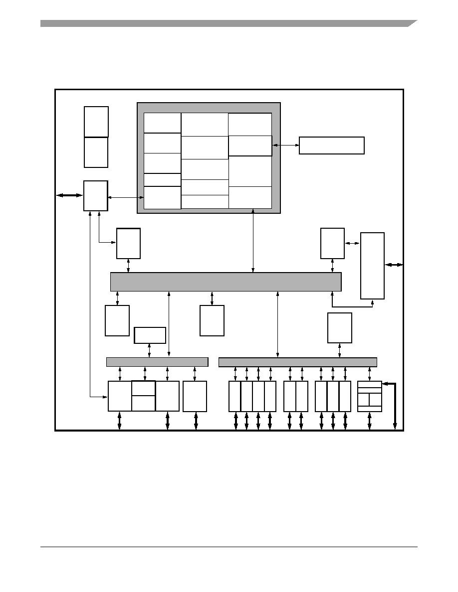
Figure 1
shows a top-level block diagram of the MPC5554.
Figure 1. MPC5554 Block Diagram
Unified 32-Kbyte
Interrupt Controller
DSPI
eS
C
I
Fl
e
x
CA
N
eQADC
FMPLL
Crossbar Switch (XBAR)
Peripheral Bridge B (PBRIDGE_B)
Peripheral Bridge A (PBRIDGE_A)
Master
Master
Master
Slave
Slave
Slave
Slave
Cache
Multiply
Unit
Load/Store Unit
Branch
Instruction
Unit
e200z6 Core
Nexus
LEGEND
JTAG
Exception
Handler
eTPU
32
channel
3K Data
RAM
16K Code
RAM
eMIOS
24
channel
DSPI
DSPI
DSPI
eS
C
I
Fl
e
x
CA
N
Fl
e
x
CA
N
Flash
2Mbyte
eDMA
64
channels
AMUX
ADC
ADCi
ADC
Exte
rnal Bu
s I
nte
rf
ace
Slave
Nexus
Interface
External
Master
Interface
eTPU
32
channel
1.5V
Regulator
Control
System/Bus
Integration
Boot
Assist
Module
MPC5500 Device Module Acronyms
CAN
≠ Controller area network (FlexCAN)
DSPI
≠ Deserial/serial peripheral interface
DMA
≠ Enhanced direct memory access
eMIOS ≠ Enhanced modular I/O system
eQADC ≠ Enhanced queued analog/digital converter
eSCI
≠ Enhanced serial communications interface
eTPU
≠ Enhanced time processing units
FMPLL ≠ Frequency modulated phase-locked loop
SRAM
≠ Static RAM
e200z6 Core Component Acronyms
DEC
≠ Decrementer
FIT
≠ Fixed interval timer
TB
≠ Time base
WDT
≠ Watchdog timer
Prediction Unit
Signal
Processing
Engine
64-bit General
Purpose
Registers
Special
Purpose
Registers
Integer
Execution
Unit
SRAM
64 Kbyte
Memory
Management
Unit
Core Timers
Unit
(FIT, TB, DEC)

MPC5554 Microcontroller Product Brief, Rev. 2.1
Features
Freescale Semiconductor
4
2
Features
This section provides a high-level description of the major features of the MPC5554.
∑
High performance e200z6 core processor
-- 32-bit PowerPC Book E compliant CPU
-- 32 64-bit general-purpose registers (GPRs)
-- Memory management unit (MMU) with 32-entry, fully-associative translation look-aside
buffer (TLB)
-- Branch processing unit
-- Fully pipelined load/store unit
-- 32-Kbyte unified cache with line locking
≠ 8-way set associative
≠ 2 32-bit fetches per clock
≠ 8-entry store buffer
≠ Way locking
≠ Supports assigning cache as instruction or data only on a per way basis
≠ Supports tag and data parity
-- Vectored interrupt support
-- Interrupt latency < 70 ns @132MHz (measured from interrupt request to execution of first
instruction of interrupt exception handler)
-- Reservation instructions for implementing read-modify-write constructs (internal SRAM and
Flash)
-- Signal processing engine (SPE) auxiliary processing unit (APU) operating on 64-bit GPRs
-- Floating point
≠ IEEE
Æ 754 compatible with software wrapper
≠ Single precision in hardware and double precision with software library
≠ Conversion instructions between single precision floating point and fixed point
-- Long cycle time instructions, except for guarded loads, do not increase interrupt latency in the
MPC5554. To reduce latency, long cycle time instructions are aborted upon interrupt requests.
-- Extensive system development support through Nexus debug module
∑
Crossbar switch (XBAR)
-- 3 master ports; 5 slave ports
-- 32-bit address bus; 64-bit data bus
-- Simultaneous accesses from different masters to different slaves (there is no clock penalty
when a parked master accesses a slave)

Features
MPC5554 Microcontroller Product Brief, Rev. 2.1
Freescale Semiconductor
5
∑
Enhanced direct memory access (eDMA) controller
-- 64 channels support independent 8-, 16-, 32-, or 64-bit single value or block transfers
-- Supports variable sized queues and circular queues
-- Source and destination address registers are independently configured to post-increment or
remain constant
-- Each transfer is initiated by a peripheral, CPU, or eDMA channel request
-- Each eDMA channel can optionally send an interrupt request to the CPU on completion of a
single value or block transfer
∑
Interrupt controller (INTC)
-- 308 total interrupt vectors
≠ 278 peripheral interrupt requests
≠ plus 8 software setable sources
≠ plus 22 reserved interrupts
-- Unique 9-bit vector per interrupt source
-- 16 priority levels with fixed hardware arbitration within priority levels for each interrupt
source
-- Priority elevation for shared resources
∑
Frequency modulated phase-locked loop (FMPLL)
-- Input clock frequency from 8 MHz to 20 MHz
-- Current controlled oscillator (ICO) range from 50 MHz to maximum device frequency
-- Reduced frequency divider (RFD) for reduced frequency operation without re-lock
-- 4 selectable modes of operation
-- Programmable frequency modulation
-- Lock detect circuitry continuously monitors lock status
-- Loss of clock (LOC) detection for reference and feedback clocks
-- Self-clocked mode (SCM) operation
-- On-chip loop filter (reduces number of external components required)
-- Engineering clock output
∑
External bus interface (EBI)
-- 1.8V
≠
3.3V I/O nominal I/O voltage
-- Memory controller with support for various memory types
-- 32-bit data bus and 24-bit address bus with transfer size indication
-- Selectable drive strength
-- Configurable bus speed modes
-- Support for external master accesses to internal addresses
-- Burst support