 | ÐлекÑÑоннÑй компоненÑ: MPC7457 | СкаÑаÑÑ:  PDF PDF  ZIP ZIP |
Äîêóìåíòàöèÿ è îïèñàíèÿ www.docs.chipfind.ru

© Freescale Semiconductor, Inc., 2004. All rights reserved.
Freescale Semiconductor
Technical Data
This hardware specification is primarily concerned with the
MPC7457; however, unless otherwise noted, all information here
also applies to the MPC7447. The MPC7457 and MPC7447 are
implementations of the PowerPCTM microprocessor family of
reduced instruction set computer (RISC) microprocessors. This
hardware specification describes pertinent electrical and physical
characteristics of the MPC7457. For functional characteristics of
the processor, refer to the MPC7450 RISC Microprocessor Family
User's Manual.
To locate any published updates for this hardware specification,
refer to the website at http://www.Freescale.com.
1
Overview
The MPC7457 is the fourth implementation of the fourth
generation (G4) microprocessors from Freescale. The MPC7457
implements the full PowerPC 32-bit architecture and is targeted at
networking and computing systems applications. The MPC7457
consists of a processor core, a 512-Kbyte L2, and an internal L3
tag and controller that support a glueless backside L3 cache
through a dedicated high-bandwidth interface. The MPC7447 is
identical to the MPC7457 except that it does not support the L3
cache interface.
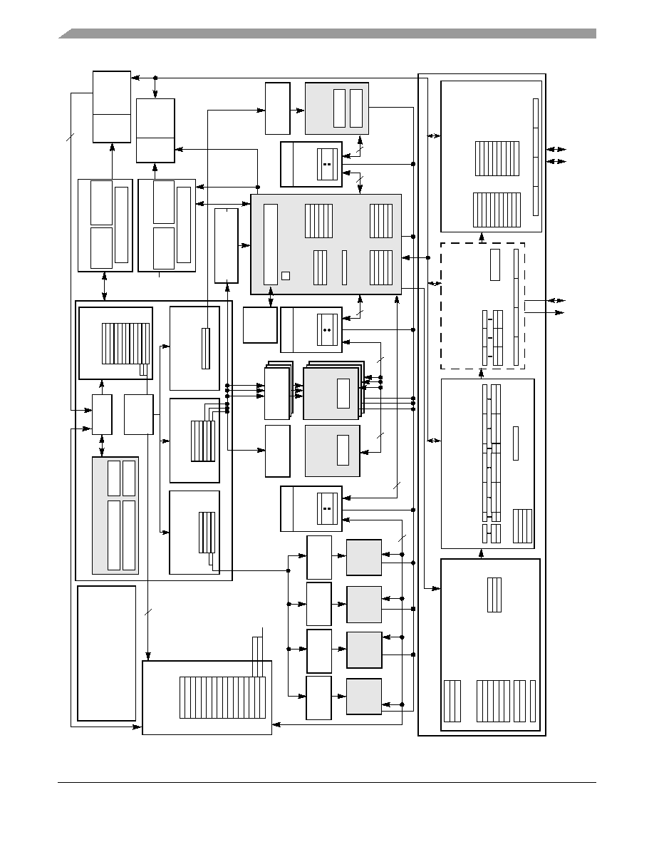
Figure 1
shows a block diagram of the MPC7457. The core is a
high-performance superscalar design supporting a
double-precision floating-point unit and a SIMD multimedia unit.
MPC7457EC
Rev. 5, 09/2004
Contents
1. Overview . . . . . . . . . . . . . . . . . . . . . . . . . . . . . . . . . . . 1
2. Features . . . . . . . . . . . . . . . . . . . . . . . . . . . . . . . . . . . . 3
3. Comparison with the MPC7455, MPC7445,
MPC7450, MPC7451, and MPC7441 . . . . . . . . . . . . 7
4. General Parameters . . . . . . . . . . . . . . . . . . . . . . . . . . 10
5. Electrical and Thermal Characteristics . . . . . . . . . . . 10
6. Pin Assignments . . . . . . . . . . . . . . . . . . . . . . . . . . . . 33
7. Pinout Listings . . . . . . . . . . . . . . . . . . . . . . . . . . . . . 35
8. Package Description . . . . . . . . . . . . . . . . . . . . . . . . . 41
9. System Design Information . . . . . . . . . . . . . . . . . . . 47
10. Document Revision History . . . . . . . . . . . . . . . . . . . 61
11. Part Numbering and Marking . . . . . . . . . . . . . . . . . . 63
MPC7457
RISC Microprocessor
Hardware Specifications
MPC7457 RISC Microprocessor Hardware Specifications, Rev. 5
2
Freescale Semiconductor
Overview
Figure 1. MPC7457 Block Diagram
+
In
t
e
g
e
r
Re
s
e
r
v
a
t
i
o
n
St
a
t
i
o
n
Un
it
2
+
In
t
e
g
e
r
R
e
s
e
r
v
ati
on
St
a
t
i
o
n
Un
it
2
A
ddi
t
i
on
a
l
Fe
a
t
u
r
e
s
· T
i
me
B
a
s
e
C
o
u
n
ter
/
D
e
c
r
em
enter
·
C
l
o
c
k
M
u
l
t
ip
lie
r
· J
T
A
G
/CO
P
Inter
f
ac
e
· T
her
mal
/
P
o
w
e
r
M
anage
ment
· P
e
r
f
o
r
m
anc
e
Moni
tor
+
+
x ÷
FP
S
C
R
FP
S
C
R
PA
+ x
÷
In
st
r
u
ct
io
n
Un
it
Ins
t
r
u
c
t
i
on Q
ueue
(1
2
-
W
o
rd
)
96-
B
i
t (
3
Ins
t
r
u
c
t
i
ons
)
R
e
s
e
r
v
ati
o
n
In
t
e
g
e
r
128-
B
i
t (
4
In
s
t
r
u
c
t
i
o
n
s
)
32
-
B
i
t
Fl
o
a
t
i
ng-
P
o
in
t
Un
it
64-
B
i
t
R
e
s
e
r
v
ati
o
n
Loa
d/
S
t
or
e
U
n
i
t
(
E
A
C
a
l
c
ul
ati
on)
F
i
n
i
s
hed
32-
B
i
t
Co
m
p
le
t
i
o
n
Un
i
t
C
o
mpl
e
ti
on
Q
u
eue
(
16-
E
n
t
r
y
)
T
ags
32
-
K
by
t
e
D Ca
c
h
e
36-
B
i
t
64
-
B
i
t
In
t
e
g
e
r
S
t
at
i
ons
(
2
)
Re
s
e
r
v
a
t
i
o
n
St
a
t
i
o
n
R
e
s
e
r
v
ati
on
S
t
at
i
o
ns
(
2
)
FP
R
F
i
l
e
16 R
e
name
Bu
f
f
e
r
s
S
t
at
i
o
ns
(
2
-
E
n
t
r
y
)
GP
R
F
i
l
e
16 R
e
name
B
u
ffer
s
R
e
s
e
r
v
ati
on
St
a
t
i
o
n
VR
F
i
le
1
6
R
enam
e
B
u
ffer
s
64-
B
i
t
12
8-
B
i
t
128
-
B
i
t
Co
m
p
l
e
t
e
s
u
p
Co
m
p
l
e
te
d
In
st
r
u
ct
i
o
n
M
M
U
SR
s
(
S
ha
dow
)
128-
E
n
tr
y
IB
A
T
A
r
r
a
y
IT
LB
Ta
g
s
32
-
K
b
y
t
e
I C
a
c
h
e
S
t
or
es
S
t
or
es
Lo
ad Mi
s
s
Ve
c
t
o
r
T
ouc
h
Qu
e
u
e
(3
)
V
R
Is
s
u
e
F
P
R
Is
s
u
e
B
r
an
ch
P
r
o
cessin
g
U
n
it
CT
R
LR
B
T
IC
(
128
-
E
ntr
y
)
B
H
T
(
2048
-
E
ntr
y
)
Fe
t
c
h
e
r
GP
R
I
s
s
u
e
(
6
-E
n
t
ry
/
3
-I
s
s
u
e
)
(4
-E
n
t
r
y
/
2
-I
s
s
u
e
)
(2
-E
n
t
ry
/
1
-
I
s
s
u
e
)
D
i
s
patc
h
Un
i
t
Da
t
a
M
M
U
SR
s
(
O
r
i
gi
nal
)
128
-
E
ntr
y
DB
A
T
A
r
r
a
y
DT
L
B
V
e
c
t
or
T
ouc
h
E
ngi
ne
32
-
B
i
t
EA
L1 C
a
s
t
o
u
t
St
a
t
u
s
L
2
S
t
o
r
e Q
u
eu
e
(
L
2S
Q
)
Ve
c
t
o
r
FP
U
Re
s
e
r
v
a
t
i
o
n
St
a
t
i
o
n
R
e
s
e
r
v
ati
o
n
St
a
t
i
o
n
R
e
s
e
r
v
at
i
on
St
a
t
i
o
n
V
ect
o
r
In
t
e
g
e
r
Un
it
1
V
ect
o
r
In
t
e
g
e
r
Un
it
2
Ve
c
t
o
r
Pe
rm
u
t
e
Un
it
Li
ne
Ta
g
s
B
l
o
ck
0 (
32-
B
y
t
e
)
St
a
t
u
s
B
l
o
c
k 1 (
32-
B
y
t
e
)
Me
m
o
r
y
S
u
b
sys
t
e
m
S
noop P
u
s
h
/
Int
e
r
v
enti
ons
L
1
C
a
s
t
outs
Bu
s
Ac
c
u
m
u
l
a
t
o
r
L1 P
u
s
h
(4
)
Un
it
2
U
n
i
t
1
to thr
ee
p
e
r
cl
o
c
k
in
s
t
r
u
ct
i
o
n
s
L1 L
oad Q
ueu
e (
LLQ
)
L
1
Load
Mi
s
s
(
5
)
C
a
c
heab
l
e
S
t
or
e
R
eque
s
t
(
1
)
Ins
t
r
u
c
t
i
on F
e
tc
h
(
2
)
L
1
S
e
r
v
ice
L
1
S
t
or
e Q
ueue
(L
S
Q
)
L
3
Cach
e Co
n
t
ro
ller
1
L3
C
R
S
t
at
us
T
ags
Bu
s Ac
cu
mu
la
t
o
r
B
l
oc
k
0/
1
Li
ne
S
y
st
em
B
u
s
I
n
t
e
r
f
ac
e
L2
P
r
efetc
h
(
3
)
64
-
B
i
t
D
a
t
a
(8
-B
i
t
P
a
ri
t
y
)
Ex
t
e
r
n
a
l
SR
A
M
A
ddr
es
s
B
u
s
Da
t
a
B
u
s
Q
u
eu
es
Ca
s
t
o
u
t
B
u
s
S
t
or
e
Q
u
eue
Pu
s
h
Load
Q
u
eue (
1
1)
Q
u
e
u
e
(9
)/
Q
u
e
ue (
10)
2
N
o
t
es:
1.
T
h
e L3 c
a
c
he i
n
ter
f
ac
e i
s
not
i
m
p
l
eme
n
ted o
n
the M
P
C
7
4
47.
2. T
he C
a
s
t
ou
t Q
u
eue an
d P
u
s
h
Q
ueu
e s
h
ar
e r
e
s
o
u
r
c
e
s
s
u
c
h
fo
r
a
c
o
m
b
i
n
ed total
of 10
entr
i
es
.
T
he C
a
s
t
out
Q
u
eue i
t
s
e
l
f
i
s
l
i
mi
ted to 9
entr
i
e
s
, e
n
s
u
r
i
ng 1 e
n
tr
y
w
i
l
l
be av
ai
l
abl
e for
a
pus
h.
5
12-
K
b
yt
e
U
n
if
ie
d
L
2
C
ach
e C
o
n
t
r
o
l
l
er
19-
B
i
t A
d
d
r
es
s
(
1
, 2, or
4 M
b
y
t
e
s
)

MPC7457 RISC Microprocessor Hardware Specifications, Rev. 5
Freescale Semiconductor
3
Features
The memory storage subsystem supports the MPX bus protocol and a subset of the 60x bus protocol to main memory
and other system resources. The L3 interface supports 1, 2, or 4 Mbytes of external SRAM for L3 cache and/or
private memory data. For systems implementing 4 Mbytes of SRAM, a maximum of 2 Mbytes may be used as cache;
the remaining 2 Mbytes must be private memory.
Note that the MPC7457 is a footprint-compatible, drop-in replacement in a MPC7455 application if the core power
supply is 1.3 V.
2
Features
This section summarizes features of the MPC7457 implementation of the PowerPC architecture.
Major features of the MPC7457 are as follows:
·
High-performance, superscalar microprocessor
-- As many as four instructions can be fetched from the instruction cache at a time.
-- As many as three instructions can be dispatched to the issue queues at a time.
-- As many as 12 instructions can be in the instruction queue (IQ).
-- As many as 16 instructions can be at some stage of execution simultaneously.
-- Single-cycle execution for most instructions
-- One instruction per clock cycle throughput for most instructions
-- Seven-stage pipeline control
·
Eleven independent execution units and three register files
-- Branch processing unit (BPU) features static and dynamic branch prediction
128-entry (32-set, four-way set associative) branch target instruction cache (BTIC), a cache of
branch instructions that have been encountered in branch/loop code sequences. If a target instruction
is in the BTIC, it is fetched into the instruction queue a cycle sooner than it can be made available
from the instruction cache. Typically, a fetch that hits the BTIC provides the first four instructions
in the target stream.
2048-entry branch history (BHT) with 2 bits per entry for 4 levels of prediction--not-taken, strongly
not-taken, taken, and strongly taken
Up to three outstanding speculative branches
Branch instructions that do not update the count register (CTR) or link register (LR) are often
removed from the instruction stream.
Eight-entry link register stack to predict the target address of Branch Conditional to Link Register
(bclr) instructions
-- Four integer units (IUs) that share 32 GPRs for integer operands
Three identical IUs (IU1a, IU1b, and IU1c) can execute all integer instructions except multiply,
divide, and move to/from special-purpose register instructions
IU2 executes miscellaneous instructions including the CR logical operations, integer multiplication
and division instructions, and move to/from special-purpose register instructions
-- Five-stage FPU and a 32-entry FPR file
Fully IEEE 754-1985 compliant FPU for both single- and double-precision operations
Supports non-IEEE mode for time-critical operations

MPC7457 RISC Microprocessor Hardware Specifications, Rev. 5
4
Freescale Semiconductor
Features
Hardware support for denormalized numbers
Thirty-two 64-bit FPRs for single- or double-precision operands
-- Four vector units and 32-entry vector register file (VRs)
Vector permute unit (VPU)
Vector integer unit 1 (VIU1) handles short-latency AltiVecTM integer instructions, such as vector add
instructions (for example, vaddsbs, vaddshs, and vaddsws)
Vector integer unit 2 (VIU2) handles longer-latency AltiVec integer instructions, such as vector
multiply add instructions (for example, vmhaddshs, vmhraddshs, and vmladduhm)
Vector floating-point unit (VFPU)
-- Three-stage load/store unit (LSU)
Supports integer, floating-point, and vector instruction load/store traffic
Four-entry vector touch queue (VTQ) supports all four architected AltiVec data stream operations
Three-cycle GPR and AltiVec load latency (byte, half-word, word, vector) with one-cycle
throughput
Four-cycle FPR load latency (single, double) with one-cycle throughput
No additional delay for misaligned access within double-word boundary
Dedicated adder calculates effective addresses (EAs)
Supports store gathering
Performs alignment, normalization, and precision conversion for floating-point data
Executes cache control and TLB instructions
Performs alignment, zero padding, and sign extension for integer data
Supports hits under misses (multiple outstanding misses)
Supports both big- and little-endian modes, including misaligned little-endian accesses
·
Three issue queues FIQ, VIQ, and GIQ can accept as many as one, two, and three instructions, respectively,
in a cycle. Instruction dispatch requires the following:
-- Instructions can be dispatched only from the three lowest IQ entries--IQ0, IQ1, and IQ2
-- A maximum of three instructions can be dispatched to the issue queues per clock cycle
-- Space must be available in the CQ for an instruction to dispatch (this includes instructions that are
assigned a space in the CQ but not in an issue queue)
·
Rename buffers
-- 16 GPR rename buffers
-- 16 FPR rename buffers
-- 16 VR rename buffers
·
Dispatch unit
-- Decode/dispatch stage fully decodes each instruction
·
Completion unit
-- The completion unit retires an instruction from the 16-entry completion queue (CQ) when all
instructions ahead of it have been completed, the instruction has finished execution, and no exceptions
are pending.
-- Guarantees sequential programming model (precise exception model)
-- Monitors all dispatched instructions and retires them in order

MPC7457 RISC Microprocessor Hardware Specifications, Rev. 5
Freescale Semiconductor
5
Features
-- Tracks unresolved branches and flushes instructions after a mispredicted branch
-- Retires as many as three instructions per clock cycle
·
Separate on-chip L1 instruction and data caches (Harvard architecture)
-- 32-Kbyte, eight-way set associative instruction and data caches
-- Pseudo least recently used (PLRU) replacement algorithm
-- 32-byte (eight-word) L1 cache block
-- Physically indexed/physical tags
-- Cache write-back or write-through operation programmable on a per-page or per-block basis
-- Instruction cache can provide four instructions per clock cycle; data cache can provide four words per
clock cycle
-- Caches can be disabled in software.
-- Caches can be locked in software.
-- MESI data cache coherency maintained in hardware
-- Separate copy of data cache tags for efficient snooping
-- Parity support on cache and tags
-- No snooping of instruction cache except for icbi instruction
-- Data cache supports AltiVec LRU and transient instructions
-- Critical double- and/or quad-word forwarding is performed as needed. Critical quad-word forwarding
is used for AltiVec loads and instruction fetches. Other accesses use critical double-word forwarding.
·
Level 2 (L2) cache interface
-- On-chip, 512-Kbyte, eight-way set associative unified instruction and data cache
-- Fully pipelined to provide 32 bytes per clock cycle to the L1 caches
-- A total nine-cycle load latency for an L1 data cache miss that hits in L2
-- PLRU replacement algorithm
-- Cache write-back or write-through operation programmable on a per-page or per-block basis
-- 64-byte, two-sectored line size
-- Parity support on cache
·
Level 3 (L3) cache interface (not implemented on MPC7447)
-- Provides critical double-word forwarding to the requesting unit
-- Internal L3 cache controller and tags
-- External data SRAMs
-- Support for 1-, 2-, and 4-Mbyte (MB) total SRAM space
-- Support for 1- or 2-MB of cache space
-- Cache write-back or write-through operation programmable on a per-page or per-block basis
-- 64-byte (1-MB) or 128-byte (2-MB) sectored line size
-- Private memory capability for half (1 MB minimum) or all of the L3 SRAM space for a total of 1-, 2-,
or 4-MB of private memory
-- Supports MSUG2 dual data rate (DDR) synchronous burst SRAMs, PB2 pipelined synchronous burst
SRAMs, and pipelined (register-register) late write synchronous burst SRAMs
-- Supports parity on cache and tags
Document Outline