
1
MRF6522-70R3
MOTOROLA RF DEVICE DATA
The RF MOSFET Line
RF Power Field Effect Transistor
N-Channel Enhancement-Mode Lateral MOSFET
Designed for GSM 900 frequency band, the high gain and broadband
performance of this device make it ideal for large - signal, common source
amplifier applications in 26 volt base station equipment.
∑ Specified Performance @ Full GSM Band, 921-960 MHz, 26 Volts
Output Power, P1dB -- 80 Watts (Typ)
Power Gain @ P1dB -- 16 dB (Typ)
Efficiency @ P1dB -- 58% (Typ)
∑ Available in Tape and Reel. R3 Suffix = 250 Units per 32 mm, 13 inch Reel.
MAXIMUM RATINGS
Rating
Symbol
Value
Unit
Drain-Source Voltage
V
DSS
65
Vdc
Gate-Source Voltage
V
GS
±20
Vdc
Drain Current -- Continuous
I
D
7
Adc
Total Device Dissipation @ T
C
= 25∞C
Derate above 25∞C
P
D
159
0.9
Watts
W/∞C
Storage Temperature Range
T
stg
- 65 to +150
∞C
Operating Junction Temperature
T
J
200
∞C
THERMAL CHARACTERISTICS
Characteristic
Symbol
Value
Unit
Thermal Resistance, Junction to Case
R
JC
1.1
∞C/W
NOTE - CAUTION - MOS devices are susceptible to damage from electrostatic charge. Reasonable precautions in handling and
packaging MOS devices should be observed.
Order this document
by MRF6522-70/D
MOTOROLA
SEMICONDUCTOR TECHNICAL DATA
MRF6522-70R3
921 - 960 MHz, 70 W, 26 V
LATERAL N-CHANNEL
RF POWER MOSFET
CASE 465D-05, STYLE 1
NI-600
Motorola, Inc. 2004
REV 6
F
r
e
e
s
c
a
l
e
S
e
m
i
c
o
n
d
u
c
t
o
r
,
I
Freescale Semiconductor, Inc.
For More Information On This Product,
Go to: www.freescale.com
n
c
.
.
.

MRF6522-70R3
2
MOTOROLA RF DEVICE DATA
ELECTRICAL CHARACTERISTICS
(T
C
= 25∞C unless otherwise noted)
Characteristic
Symbol
Min
Typ
Max
Unit
OFF CHARACTERISTICS
Drain-Source Breakdown Voltage
(V
GS
= 0 Vdc, I
D
= 20 µAdc)
V
(BR)DSS
65
--
--
Vdc
Zero Gate Voltage Drain Current
(V
DS
= 28 Vdc, V
GS
= 0 Vdc)
I
DSS
--
--
10
µAdc
Gate-Source Leakage Current
(V
GS
= 20 Vdc, V
DS
= 0 Vdc)
I
GSS
--
--
1
µAdc
ON CHARACTERISTICS
Gate Threshold Voltage
(V
DS
= 10 Vdc, I
D
= 300 µAdc)
V
GS(th)
2
3
4
Vdc
Gate Quiescent Voltage
(V
DS
= 26 Vdc, I
D
= 400 mAdc)
V
GS(Q)
3
4
5
Vdc
Drain-Source On-Voltage
(V
GS
= 10 Vdc, I
D
= 1 Adc)
V
DS(on)
--
0.15
0.6
Vdc
Forward Transconductance
(V
DS
= 10 Vdc, I
D
= 2 Adc)
g
fs
2
3
--
S
DYNAMIC CHARACTERISTICS
Input Capacitance (1)
(V
DS
= 26 Vdc, V
GS
= 0, f = 1 MHz)
C
iss
--
130
--
pF
Output Capacitance
(V
DS
= 26 Vdc, V
GS
= 0, f = 1 MHz)
C
oss
41
47
52
pF
Reverse Transfer Capacitance
(V
DS
= 26 Vdc, V
GS
= 0, f = 1 MHz)
C
rss
2.4
3
3.4
pF
FUNCTIONAL TESTS (In Motorola Test Fixture)
Output Power (2)
(V
DD
= 26 Vdc, I
DQ
= 400 mA, f = Full GSM Band 921 - 960 MHz)
P1dB
73
80
--
W
Common-Source Amplifier Power Gain @ P1dB (Min) (2)
(V
DD
= 26 Vdc, I
DQ
= 400 mA, f = Full GSM Band 921 - 960 MHz)
G
ps
14
16
18
dB
Drain Efficiency @ P
out
= 50 W
(V
DD
= 26 Vdc, I
DQ
= 400 mA, f = Full GSM Band 921 - 960 MHz)
1
47
51
--
%
Drain Efficiency @ P1dB (2)
(V
DD
= 26 Vdc, I
DQ
= 400 mA, f = Full GSM Band 921 - 960 MHz)
2
--
58
--
%
Input Return Loss @ P
out
= 50 W
(V
DD
= 26 Vdc, I
DQ
= 400 mA,
f = 921 MHz and 960 MHz
f = 940 MHz)
IRL
--
--
--
--
- 10
- 15
dB
Output Mismatch Stress (2)
(V
DD
= 26 Vdc, I
DQ
= 400 mA, f = Full GSM Band 921 - 960 MHz,
VSWR = 5:1, All Phase Angles)
No Degradation In Output Power
Before and After Test
(1) Value excludes the input matching.
(2) To meet application requirements, Motorola test fixtures have been designed to cover full GSM 900 band ensuring batch-to-batch
consistency.
F
r
e
e
s
c
a
l
e
S
e
m
i
c
o
n
d
u
c
t
o
r
,
I
Freescale Semiconductor, Inc.
For More Information On This Product,
Go to: www.freescale.com
n
c
.
.
.

3
MRF6522-70R3
MOTOROLA RF DEVICE DATA
Figure 1. MRF6522-70 Test Circuit Schematic
R6
R2
R1
C6
C5
C13
C11
C9
C8
C14
C2
Q1
C10
VSUPPLY
RF Output
C12
C3
C4
C7
RF Input
R3
R4
T2
C1
VBIAS
Vreg
T1
Gnd
Vin
Vout
C1
1.0 µF Chip Capacitor (0805)
C2
10 µF, 35 Vdc Tantalum Capacitor
C3
100 nF Chip Capacitor
C4, C6, C14 22 pF Chip Capacitors, ACCU-P (0805)
C5
2.7 pF Chip Capacitor, ACCU-P (0805)
C7, C8, C13 4.7 pF Chip Capacitors, ACCU-P (0805)
C9, C10
8.2 pF Chip Capacitors, ACCU-P (0805)
C11, C12
2.2 pF Chip Capacitors, ACCU-P (0805)
R1
10 Chip Resistor (0805)
R2
1.0 k Chip Resistor (0805)
R3
1.2 k Chip Resistor (0805)
R4
2.2 k Chip Resistor (0805)
R5
220 Chip Resistor (0805)
R6
5.0 k SMD Potentiometer
T1
LP2951 Micro-8
T2
BC847 SOT-23
SUBSTRATE GI180 0.8 mm
R5
+
Figure 2. MRF6522-70 Test Circuit Component Layout
R6
C1
R2
R1
C3
C4
C7
R5
C6
C5
C8
C9
C10
C11
C12
C13
C2
T2
STRAP
V
Ground
V
R4
C14
R3
T1
MRF6522
-
70
Q1
SUPPLY
BIAS
F
r
e
e
s
c
a
l
e
S
e
m
i
c
o
n
d
u
c
t
o
r
,
I
Freescale Semiconductor, Inc.
For More Information On This Product,
Go to: www.freescale.com
n
c
.
.
.
MRF6522-70R3
4
MOTOROLA RF DEVICE DATA
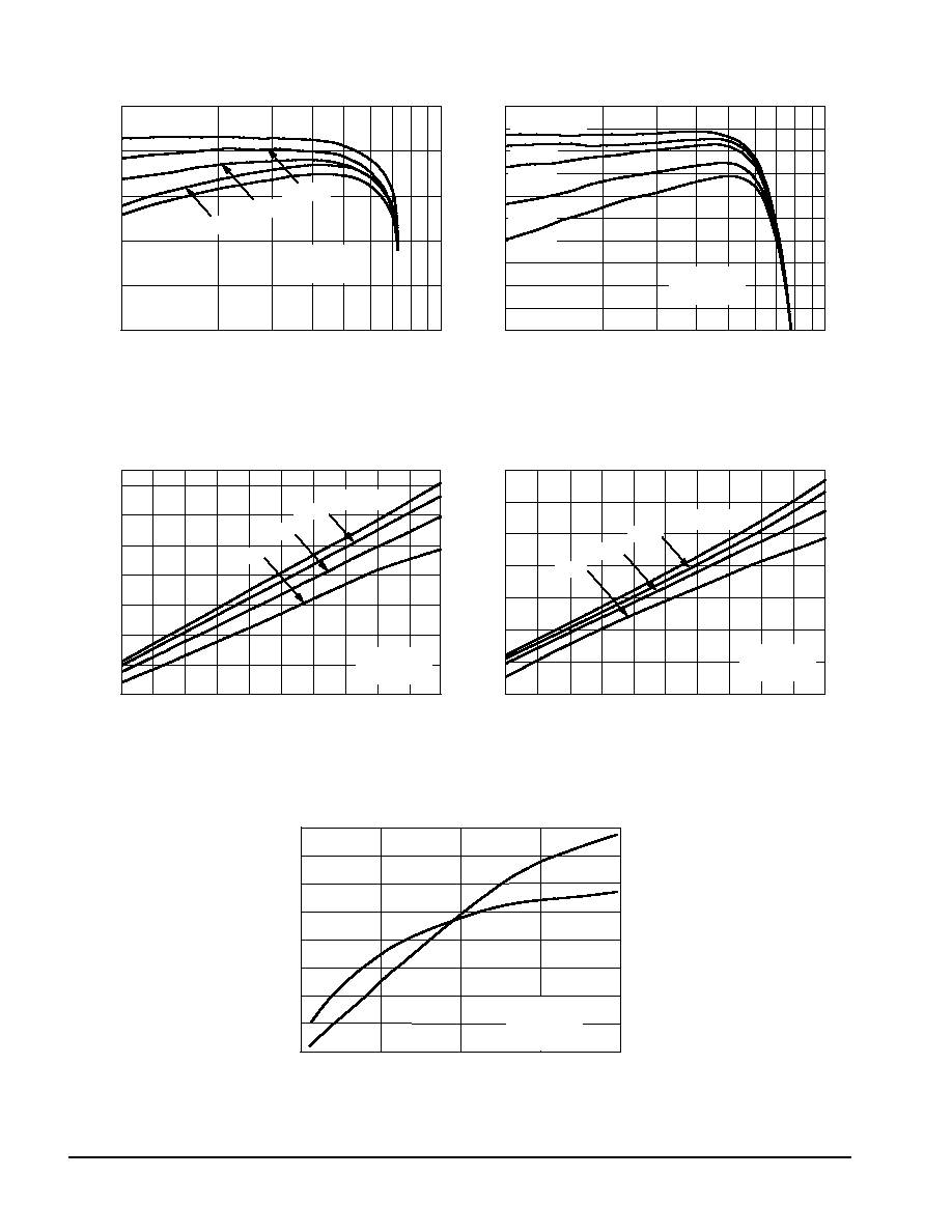
TYPICAL CHARACTERISTICS
P
out
, OUTPUT POWER (WATTS)
P
out
, OUTPUT POWER (WATTS)
17.5
15.0
Figure 3. Power Gain versus Output Power
10
15.5
16.0
Figure 4. Power Gain versus Output Power
100
10
18.0
17.6
16.2
16.6
17.4
16.0
16.5
17.0
100
G
ps
, POWER GAIN (dB)
V
DS
= 26 Vdc
f = 921 MHz
Figure 5. Output Power versus Supply Voltage
Figure 6. Output Power versus Supply Voltage
Figure 7. Efficiency and Output Power
versus Input Power
200 mA
300 mA
400 mA
500 mA
I
DQ
= 600 mA
16.4
16.8
17.2
17.0
17.8
V
DS
= 26 Vdc
f = 960 MHz
200 mA
300 mA
400 mA
500 mA
I
DQ
= 600 mA
G
ps
, POWER GAIN (dB)
V
DD
, SUPPLY VOLTAGE (VOLTS)
115
45
18
55
75
85
105
28
P out
,
OUTPUT
POWER (W
A
TTS)
20
22
24
26
65
95
I
DQ
= 400 mA
f = 921 MHz
P
in
= 5.0 W
3.0 W
4.0 W
2.0 W
V
DD
, SUPPLY VOLTAGE (VOLTS)
105
18
55
75
85
95
28
P out
,
OUTPUT
POWER (W
A
TTS)
20
22
24
26
45
65
I
DQ
= 400 mA
f = 960 MHz
P
in
= 5.0 W
3.0 W
4.0 W
2.0 W
35
h
P
in
, INPUT POWER (WATTS)
80
0
20
40
50
70
2.0
h
, EFFICIENCY
(%)
0.5
1.0
1.5
10
30
60
V
DS
= 26 Vdc
I
DQ
= 400 mA
f = 921 MHz
0
80
70
60
50
40
30
20
10
0
P out
,
OUTPUT
POWER (W
A
TTS)
P
out
19
21
23
25
27
27
19
21
23
25
F
r
e
e
s
c
a
l
e
S
e
m
i
c
o
n
d
u
c
t
o
r
,
I
Freescale Semiconductor, Inc.
For More Information On This Product,
Go to: www.freescale.com
n
c
.
.
.

5
MRF6522-70R3
MOTOROLA RF DEVICE DATA
TYPICAL CHARACTERISTICS
h
P
in
, INPUT POWER (WATTS)
Figure 8. Efficiency and Output Power
versus Input Power
0
Figure 9. Power Gain and Efficiency
versus Input Power
70
10
30
Figure 10. Power Gain and Efficiency
versus Input Power
20
40
50
60
20
19
h
, EFFICIENCY
(%)
G
ps
, POWER GAIN (dB)
18
17
16
15
14
13
V
DS
= 26 Vdc
f = 921 MHz
h
G
ps
P
in
, INPUT POWER (WATTS)
80
0
20
40
50
70
2.0
h
, EFFICIENCY
(%)
0.5
1.0
1.5
10
30
60
V
DS
= 26 Vdc
I
DQ
= 400 mA
f = 960 MHz
0
80
70
60
50
40
30
20
10
0
P out
,
OUTPUT
POWER (W
A
TTS)
P
out
3.96
2.26
1.26
0.70
0.38
0.21
0.12
0.06
0.03
0.02
P
in
, INPUT POWER (WATTS)
0
70
10
30
20
40
50
60
20
19
h
, EFFICIENCY
(%)
G
ps
, POWER GAIN (dB)
18
17
16
15
14
13
V
DS
= 26 Vdc
f = 960 MHz
h
G
ps
3.70
2.14
1.15
0.62
0.34
0.18
0.10
0.05
0.03
0.02
F
r
e
e
s
c
a
l
e
S
e
m
i
c
o
n
d
u
c
t
o
r
,
I
Freescale Semiconductor, Inc.
For More Information On This Product,
Go to: www.freescale.com
n
c
.
.
.
MRF6522-70R3
6
MOTOROLA RF DEVICE DATA
TYPICAL CHARACTERISTICS
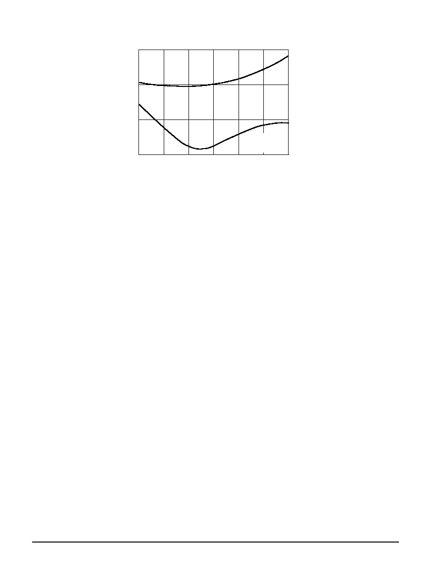
Figure 11. Performance in Broadband Circuit (at Small Signal)
f, FREQUENCY (MHz)
-10
-25
910
-20
-15
970
V
DS
= 26 Vdc
I
DQ
= 400 mA
920
950
960
IRL,
INPUT
RETURN LOSS (dB)
17
16
15
G
ps
, GAIN (dB)
18
930
940
IRL
G
ps
F
r
e
e
s
c
a
l
e
S
e
m
i
c
o
n
d
u
c
t
o
r
,
I
Freescale Semiconductor, Inc.
For More Information On This Product,
Go to: www.freescale.com
n
c
.
.
.

7
MRF6522-70R3
MOTOROLA RF DEVICE DATA
Figure 12. Series Equivalent Source and Load Impedance
f
MHz
Z
source
Z
load
925
940
960
2.65 - j2.53
2.85 - j1.87
2.67 - j2.14
1.62 + j0.2
1.56 + j0.34
1.55 + j0.2
V
SUPPLY
= 26 Vdc, I
BIAS
= 400 mA, CW = Room Temperature
Z
o
= 5
f = 925 MHz
f = 925 MHz
960 MHz
Z
source
= Test circuit impedance as measured from
gate to ground.
Z
load
= Test circuit impedance as measured
from drain to ground.
Z source
Z load
Input
Matching
Network
Device
Under Test
Output
Matching
Network
Z
source
Z
load
960 MHz
F
r
e
e
s
c
a
l
e
S
e
m
i
c
o
n
d
u
c
t
o
r
,
I
Freescale Semiconductor, Inc.
For More Information On This Product,
Go to: www.freescale.com
n
c
.
.
.
MRF6522-70R3
8
MOTOROLA RF DEVICE DATA
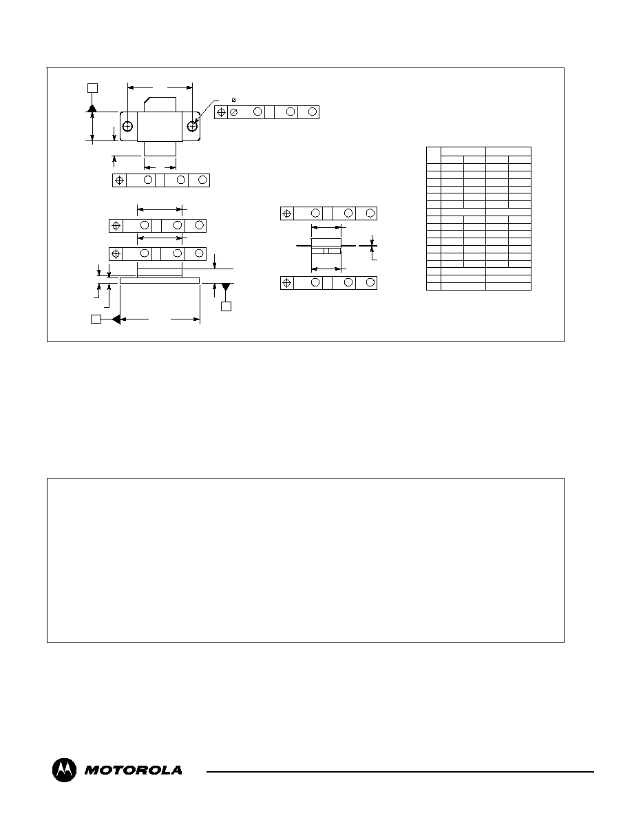
PACKAGE DIMENSIONS
CASE 465D-05
ISSUE D
NI-600
D
G
1
2
3
K
A
C
H
E
SEATING
PLANE
F
NOTES:
1. INTERPRET DIMENSIONS AND TOLERANCES
PER ANSI Y14.5M-1994.
2. CONTROLLING DIMENSION: INCH.
3. DIMENSION H IS MEASURED 0.030 (0.762) AWAY
FROM PACKAGE BODY.
DIM
MIN
MAX
MIN
MAX
MILLIMETERS
INCHES
A
1.065
1.075
27.05
27.30
B
0.380
0.390
9.65
9.91
C
0.160
0.205
4.06
5.21
D
0.425
0.435
10.80
11.05
E
0.060
0.070
1.52
1.78
F
0.004
0.006
0.10
0.15
G
0.870 BSC
22.10 BSC
H
0.096
0.106
2.44
2.69
K
0.190
0.223
4.83
5.66
M
0.594
0.606
15.09
15.39
Q
0.124
0.130
3.15
3.30
R
0.394
0.404
10.01
10.26
STYLE 1:
PIN 1. DRAIN
2. GATE
3. SOURCE
Q
2X
M
A
M
bbb
B
M
T
M
A
M
bbb
B
M
T
B
B
(FLANGE)
M
A
M
ccc
B
M
T
M
A
M
bbb
B
M
T
A
T
N
(LID)
M
(INSULATOR)
S
M
A
M
aaa
B
M
T
(INSULATOR)
R
M
A
M
ccc
B
M
T
(LID)
S
0.395
0.405
10.03
10.29
N
0.591
0.601
15.01
15.27
aaa
0.005 REF
0.13 REF
bbb
0.010 REF
0.25 REF
ccc
0.015 REF
0.38 REF
Information in this document is provided solely to enable system and software implementers to use Motorola products. There are no express or implied copyright
licenses granted hereunder to design or fabricate any integrated circuits or integrated circuits based on the information in this document.
Motorola reserves the right to make changes without further notice to any products herein. Motorola makes no warranty, representation or guarantee regarding
the suitability of its products for any particular purpose, nor does Motorola assume any liability arising out of the application or use of any product or circuit, and
specifically disclaims any and all liability, including without limitation consequential or incidental damages. "Typical" parameters that may be provided in Motorola
data sheets and/or specifications can and do vary in different applications and actual performance may vary over time. All operating parameters, including
"Typicals", must be validated for each customer application by customer's technical experts. Motorola does not convey any license under its patent rights nor the
rights of others. Motorola products are not designed, intended, or authorized for use as components in systems intended for surgical implant into the body, or other
applications intended to support or sustain life, or for any other application in which the failure of the Motorola product could create a situation where personal injury
or death may occur. Should Buyer purchase or use Motorola products for any such unintended or unauthorized application, Buyer shall indemnify and hold Motorola
and its officers, employees, subsidiaries, affiliates, and distributors harmless against all claims, costs, damages, and expenses, and reasonable attorney fees
arising out of, directly or indirectly, any claim of personal injury or death associated with such unintended or unauthorized use, even if such claim alleges that
Motorola was negligent regarding the design or manufacture of the part.
MOTOROLA and the Stylized M Logo are registered in the US Patent and Trademark Office. All other product or service names are the property of their respective
owners. Motorola, Inc. is an Equal Opportunity/Affirmative Action Employer.
E Motorola Inc. 2004
HOW TO REACH US:
USA/EUROPE/LOCATIONS NOT LISTED:
JAPAN: Motorola Japan Ltd.; SPS, Technical Information Center,
Motorola Literature Distribution
3-20-1, Minami-Azabu, Minato-ku, Tokyo 106-8573, Japan
P.O. Box 5405, Denver, Colorado 80217
81-3-3440-3569
1-800-521-6274 or 480-768-2130
ASIA/PACIFIC: Motorola Semiconductors H.K. Ltd.; Silicon Harbour Centre,
2 Dai King Street, Tai Po Industrial Estate, Tai Po, N.T., Hong Kong
852-26668334
HOME PAGE: http://motorola.com/semiconductors
MRF6522-70/D
F
r
e
e
s
c
a
l
e
S
e
m
i
c
o
n
d
u
c
t
o
r
,
I
Freescale Semiconductor, Inc.
For More Information On This Product,
Go to: www.freescale.com
n
c
.
.
.