
1
Item
Symbol
Rating
Unit
Drain-source voltage
V
DS
1000
Continuous drain current
I
D
±7
Pulsed drain current
I
D(puls]
±28
Gate-source voltage
V
GS
±30
Repetitive or non-repetitive
I
AR *2
7
Maximum Avalanche Energy
E
AV *1
463
Max. power dissipation
P
D
255
Operating and storage
T
ch
+150
temperature range
T
stg
Electrical characteristics (T
c
=25∞C unless otherwise specified)
Thermalcharacteristics
2SK3337-01
FUJI POWER MOS-FET
N-CHANNEL SILICON POWER MOS-FET
Features
High speed switching
Low on-resistance
No secondary breadown
Low driving power
Avalanche-proof
Applications
Switching regulators
UPS (Uninterruptible Power Supply)
DC-DC converters
Equivalent circuit schematic
Maximum ratings and characteristic
Absolute maximum ratings
(Tc=25∞C unless otherwise specified)
Gate(G)
Source(S)
Drain(D)
Item
Symbol Test Conditions
Zero gate voltage drain current I
DSS
V
DS
=1000V
V
GS
=±30V
I
D
=3.5A V
GS
=10V
I
D
=3.5A V
DS
=25V
V
CC
=600V I
D
=7A
V
GS
=10V
R
GS
=10
Min. Typ. Max. Units
V
V
µA
mA
nA
S
pF
nC
A
V
µs
µC
ns
Min. Typ. Max. Units
Thermal resistance
R
th(ch-c)
channel to case
R
th(ch-a)
channel to ambient
0.490
50.0
∞C/W
∞C/W
Symbol
V
(BR)DSS
V
GS(th)
I
GSS
R
DS(on)
g
fs
C
iss
C
oss
C
rss
td
(on)
t
r
td
(off)
t
f
Q
G
Q
GS
Q
GD
I
AV
V
SD
t
rr
Q
rr
Item
Drain-source breakdown voltaget
Gate threshold voltage
Gate-source leakage current
Drain-source on-state resistance
Forward transcondutance
Input capacitance
Output capacitance
Reverse transfer capacitance
Turn-on time t
on
Turn-off time t
off
Total gate charge
Gate-Source charge
Gete-Drain charge
Avalanche capability
Diode forward on-voltage
Reverse recovery time
Reverse recovery charge
Test Conditions
I
D
=1mA V
GS
=0V
I
D
=1mA V
DS
=V
GS
T
ch
=25∞C
V
GS
=0V T
ch
=125∞C
V
DS
=0V
V
DS
=25V
V
GS
=0V
f=1MHz
Vcc=500V
I
D
=7A
V
GS
=10V
L=17.3 mH T
ch
=25∞C
I
F
=2xI
DR
V
GS
=0V T
ch
=25∞C
I
F
=I
DR
V
GS
=0V
-di/dt=100A/µs T
ch
=25∞C
V
A
A
V
A
mJ
W
∞C
∞C
*1 L=17.3mH, Vcc=100V *2 Tch=150∞C
100
2.5
3.0
3.5
10
500
0.2
1.0
10
100
1.54
2.0
2.7
5.5
1480
2220
170
255
75
113
25
38
50
75
160
240
70
105
84
126
23
35
31
47
7
1.00
1.50
1.6
15.0
-55 to +150
<
2
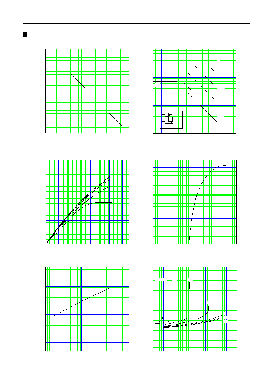
Characteristics
2SK3337-01
FUJI POWER MOSFET
0
25
50
75
100
125
150
0
50
100
150
200
250
300
Allowable Power Dissipation
PD=f(Tc)
PD [W]
Tc [∞C]
10
1
10
2
10
3
10
-1
10
0
10
1
10
2
100ms
10ms
1ms
100µs
10µs
Safe operating area
ID=f(VDS):Single Pulse,Tc=25∞C
t=
1µs
D.C.
ID [A]
VDS [V]
0
2
4
6
8
10
12
14
16
18
20
22
24
26
0
2
4
6
8
10
12
14
20V
10V
7V
6.0V
5.5V
5.0V
ID [A]
VDS [V]
Typical Output Characteristics
ID=f(VDS):80µs pulse test,Tch=25∞C
VGS=4.5V
0
1
2
3
4
5
6
7
8
0.01
0.1
1
10
ID[A]
VGS[V]
Typical Transfer Characteristic
ID=f(VGS):80µs pulse test,VDS=25V,Tch=25∞C
0.1
1
10
0.1
1
10
gfs [S]
ID [A]
Typical Transconductance
gfs=f(ID):80µs pulse test,VDS=25V,Tch=25∞C
0
2
4
6
8
10
12
14
16
0
1
2
3
4
5
RDS(on) [
]
ID [A]
Typical Drain-Source on-state Resistance
RDS(on)=f(ID):80µs pulse test,Tch=25∞C
10V
20V
7V
6.0V
5.5V
5.0V
VGS=4.5V
t
T
D=
t
T

3
10
-1
10
0
10
1
10
1
10
2
10
3
Typical Switching Characteristics vs. ID
t=f(ID):Vcc=600V,VGS=10V,RG=10
td(on)
tr
tf
td(off)
t [ns]
ID [A]
2SK3337-01
FUJI POWER MOSFET
-50
-25
0
25
50
75
100
125
150
0
1
2
3
4
5
6
7
8
RDS(on) [
]
Tch [∞C]
typ.
max.
Drain-Source On-state Resistance
RDS(on)=f(Tch):ID=3.5A,VGS=10V
-50
-25
0
25
50
75
100
125
150
0.0
0.5
1.0
1.5
2.0
2.5
3.0
3.5
4.0
4.5
5.0
max.
typ.
min.
Gate Threshold Voltage vs. Tch
VGS(th)=f(Tch):VDS=VGS,ID=1mA
VGS(th) [V]
Tch [∞C]
0
50
100
150
200
0
5
10
15
20
25
Qg [C]
Typical Gate Charge Characteristics
VGS=f(Qg):ID=7A,Tch=25∞C
VGS [V]
800V
500V
Vcc= 200V
10
-2
10
-1
10
0
10
1
10
2
10
-11
10
-10
10
-9
10
-8
10
-7
C [F]
VDS [V]
Typical Capacitance
C=f(VDS):VGS=0V,f=1MHz
Crss
Coss
Ciss
0.00
0.25
0.50
0.75
1.00
1.25
1.50
0.1
1
10
100
IF [A]
VSD [V]
Typical Forward Characteristics of Reverse Diode
IF=f(VSD):80µs pulse test,Tch=25∞C
4
10
-5
10
-4
10
-3
10
-2
10
-1
10
0
10
1
10
-3
10
-2
10
-1
10
0
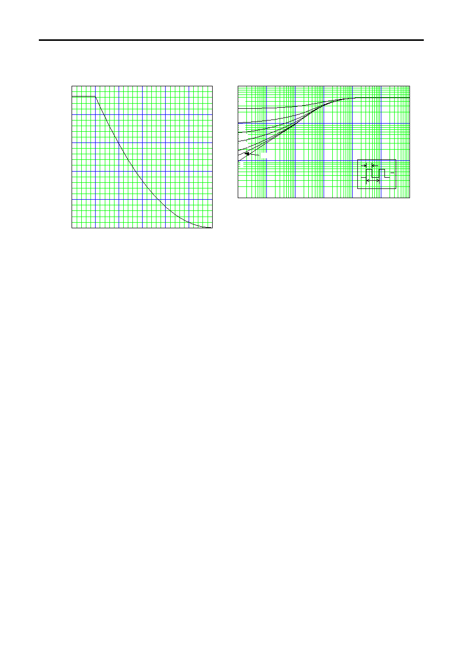
Transient Thermal impedance
Zth(ch-c)=f(t) parameter:D=t/T
Zth(ch-c) [K/W]
t [s]
0.5
0.2
0.02
0.05
0.1
0.01
0
2SK3337-01
FUJI POWER MOSFET
0
25
50
75
100
125
150
0
100
200
300
400
500
EAV [mJ]
starting Tch [∞C]
Maximum Avalanche Energy vs. starting Tch
E(AV)=f(starting Tch):Vcc=100V,I(AV)<=7A
t
T
D=
t
T