6MBI100S-120
IGBT Modules
IGBT MODULE ( S series)
1200V / 100A 6 in one-package
Features
∑ Compact package
∑ P.C.board mount
∑ Low V
CE
(sat)
Applications
∑ Inverter for motor drive
∑ AC and DC servo drive amplifier
∑ Uninterruptible power supply
∑ Industrial machines, such as welding machines
Maximum ratings and characteristics
Absolute maximum ratings (Tc=25∞C unless otherwise specified)
Item Symbol
Collector-Emitter voltage V
CES
Gate-Emitter voltage V
GES
Collector Continuous Tc=25∞C I
C
current Tc=80∞C
1ms
Tc=25∞C I
C
pulse
Tc=80∞C
-I
C
1ms -I
C
pulse
Max. power dissipation (1 device) P
C
Operating temperature
T
j
Storage temperature T
stg
Isolation voltage V
is
Screw torque Mounting *
1
Rating
1200
±20
150
100
300
200
100
200
700
+150
-40 to +125
AC 2500 (1min.)
3.5
Unit
V
V
A
A
A
A
W
∞C
∞C
V
N∑m
Item Symbol Characteristics Conditions Unit
Min. Typ. Max.
Zero gate voltage collector current
Gate-Emitter leakage current
Gate-Emitter threshold voltage
Collector-Emitter saturation voltage
Input capacitance
Output capacitance
Reverse transfer capacitance
Turn-on time
Turn-off time
Diode forward on voltage
Reverse recovery time
I
CES
I
GES
V
GE(th)
V
CE(sat)
C
ies
C
oes
C
res
t
on
t
r
t
r(i)
t
off
t
f
V
F
t
rr
≠ ≠ 1.0
≠ ≠ 0.2
5.5 7.2 8.5
≠ 2.3 2.6
≠ 2.8 ≠
≠ 12000 ≠
≠ 2500 ≠
≠ 2200 ≠
≠ 0.35 1.2
≠ 0.25 0.6
≠ 0.1 ≠
≠ 0.45 1.0
≠ 0.08 0.3
≠ 2.5 3.3
≠ 2.0 ≠
≠ ≠ 0.35
V
GE
=0V, V
CE
=1200V
V
CE
=0V, V
GE
=±20V
V
CE
=20V, I
C
=100mA
Tj=25∞C V
GE
=15V, I
C
=100A
Tj=125∞C
V
GE
=0V
V
CE
=10V
f=1MHz
V
CC
=600V
I
C
=100A
V
GE
=±15V
R
G
=12
Tj=25∞C I
F
=100A, V
GE
=0V
Tj=125∞C
I
F
=100A
mA
µA
V
V
pF
µs
V
µs
Electrical characteristics (Tj=25∞C unless otherwise specified)
Thermal resistance characteristics
Item Symbol Characteristics Conditions Unit
Min. Typ. Max.
Rth(j-c)
Thermal resistance Rth(j-c)
Rth(c-f)*
2
≠ ≠ 0.18
≠ ≠ 0.36
≠ 0.05 ≠
IGBT
FWD
the base to cooling fin
∞C/W
∞C/W
∞C/W
*
2
:
This is the value which is defined mounting on the additional cooling fin with thermal compound
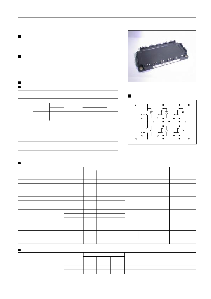
Equivalent Circuit Schematic
*
1 :
Recommendable value : 2.5 to 3.5 N∑m (M5)
21(P)
20(N)
1(Gu)
2(Eu)
3(Gx)
5(Gv)
6(Ev)
19(U)
7(Gy)
17(V)
15(W)
9(Gw)
11(Gz)
10(Ew)
4(Ex)
8(Ey)
12(Ez)
13(P)
14(N)

6MBI100S-120
IGBT Modules
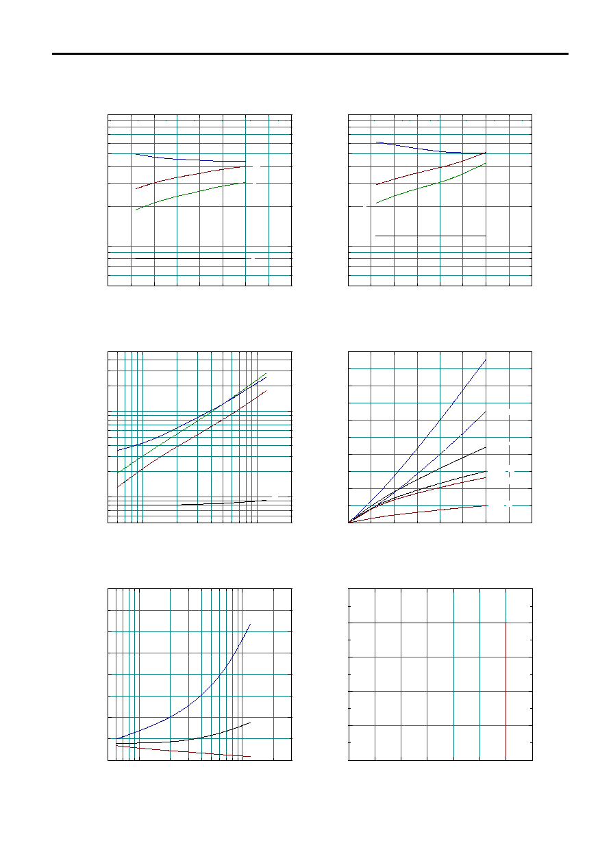
Characteristics
0
1
2
3
4
5
0
50
100
150
200
250
8V
10V
12V
15V
VGE= 20V
Collector current vs. Collector-Emitter voltage
Tj= 25
o
C (typ.)
Collector current : Ic [ A ]
Collector - Emitter voltage : VCE [ V ]
0
1
2
3
4
5
0
50
100
150
200
250
8V
10V
12V
15V
VGE= 20V
Collector current vs. Collector-Emitter voltage
Tj= 125
o
C (typ.)
Collector - Emitter voltage : VCE [ V ]
Collector current : Ic [ A ]
0
1
2
3
4
5
0
50
100
150
200
250
Tj= 25
o
C
Tj= 125
o
C
Collector current vs. Collector-Emitter voltage
VGE=15V (typ.)
Collector - Emitter voltage : VCE [ V ]
Collector current : Ic [ A ]
5
10
15
20
25
0
2
4
6
8
10
Ic= 50A
Ic= 100A
Ic= 200A
Collector-Emitter voltage vs. Gate-Emitter voltage
Tj= 25
o
C (typ.)
Collector - Emitter voltage : VCE [ V ]
Gate - Emitter voltage : VGE [ V ]
0
5
10
15
20
25
30
35
500
1000
10000
50000
Capacitance vs. Collector-Emitter voltage (typ.)
VGE=0V, f= 1MHz, Tj= 25
o
C
Capacitance : Cies, Coes, Cres [ pF ]
Collector - Emitter voltage : VCE [ V ]
Coes
Cres
Cies
0
200
400
600
800
1000
0
200
400
600
800
1000
Dynamic Gate charge (typ.)
Vcc=600V, Ic=100A, Tj= 25
o
C
Gate charge : Qg [ nC ]
Collector - Emitter voltage : VCE [ V ]
0
5
10
15
20
25
Gate - Emitter voltage : VGE [ V ]
6MBI100S-120
IGBT Modules
Vcc=600V,V
GE=
±15V, Rg=12
,Tj=125
o
C
Vcc=600V,V
GE=
±15V, Rg=12
,Tj=25
o
C
+V
GE
=15V,-V
GE<
15V, Rg>12
,Tj<125
o
C
=
=
=
Vcc=600V,Ic=100A,V
GE=
±15V ,Tj=125
o
C
Vcc=600V,Ic=100A,V
GE=
±15V,Tj=25
o
C
Vcc=600V,V
GE=
±15V, Rg=12
,Tj=125
o
C
0
50
100
150
200
50
100
500
1000
ton
tr
toff
tf
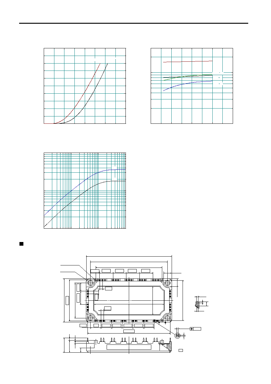
Switching time vs. Collector current (typ.)
Switching time : ton, tr, toff, tf [ nsec ]
Collector current : Ic [ A ]
0
50
100
150
200
50
100
500
1000
tf
tr
ton
toff
Switching time vs. Collector current (typ.)
Collector current : Ic [ A ]
Switching time : ton, tr, toff, tf [ nsec ]
10
50
100
200
50
100
500
1000
5000
toff
ton
tr
Switching time vs. Gate resistance (typ.)
Gate resistance : Rg [
]
Switching time : ton, tr, toff, tf [ nsec ]
0
50
100
150
200
0
5
10
15
20
25
Err(25
o
C)
Eoff(25
o
C)
Eon(25
o
C)
Err(125
o
C)
Eoff(125
o
C)
Eon(125
o
C)
Switching loss vs. Collector current (typ.)
Switching loss : Eon, Eoff, Err [ mJ/pulse ]
Collector current : Ic [ A ]
10
50
100
300
0
20
40
60
80
Switching loss vs. Gate resistance (typ.)
Switching loss : Eon, Eoff, Err [ mJ/pulse ]
Gate resistance : Rg [
]
Eon
Err
Eoff
0
200
400
600
800
1000
1200
1400
0
50
100
150
200
250
Reverse bias safe operating area
Collector - Emitter voltage : VCE [ V ]
Collector current : Ic [ A ]
6MBI100S-120
IGBT Modules
Vcc=600V,V
GE=
±15V, Rg=12
,Tj=25
o
C
12
11
9
8
7
6
5
4
3
2
1
21
20
19
18
17
16 15
14
13
122
±
1
110
±
0.3
94.5
±
0.3
99.6
±
0.3
13.09
19.05
19.05
15.24
15.24 15.24
118.11
15.24
15
15.24
19.05
19.05
8-R2.25
±
0.3
4-¯5.5
±
0.3
62
±
1
58.42
50
±
0.3
57.5
±
0.3
39.9
±
0.3
19.05
3.81
3.81
3.81
11.67
4.06
1.15
±
0.2
¯2.5
±
0.1
¯2.1
±
0.1
20.5
±
1
17
±
1
3.5
±
0.5
2.5
±
0.3
1.5
±
0.3
6.5
±
0.5
1
±
0.2
0.8
±
0.2
6
1.5
Section A-A
A
A
¯0.4
11.5
+0.5
0
11.5
+0.5
0
Shows theory dimensions
M626
Outline Drawings, mm
0
1
2
3
4
0
50
100
150
200
250
Tj=25
o
C
Tj=125
o
C
Forward current vs. Forward on voltage (typ.)
Forward current : IF [ A ]
Forward on voltage : VF [ V ]
0
50
100
150
200
10
100
300
Irr(125
o
C)
Irr(25
o
C)
trr(25
o
C)
trr(125
o
C)
Reverse recovery characteristics (typ.)
Forward current : IF [ A ]
Reverse recovery current : Irr [ A ]
Reverse recovery time : trr [ nsec ]
0.001
0.01
0.1
1
0.01
0.1
1
Transient thermal resistance
Thermal resistanse : Rth(j-c) [
o
C/W ]
Pulse width : Pw [ sec ]
FWD
IGBT