
1. Gate
2. Drain
3. Source
20 Min
15.5
5.5
9.3
5.45
5.45
5.5
3.2
21.5
1.6
3.5
1.1
2.1
2.3
0.6
Ī
0.2
Ī
0.2
Ī
0.3
Ī
0.3
Ī
0.3
Ī
0.3
Ī
0.2
Ī
0.2
Ī
0.2
Ī
0.3
Ī
0.3
+0.2
+0.3
+0.2
--0.1
Ī
0.2
Ý3.2
ESAC83M-004R
(20A)
(40V / 20A )
Features
Insulated package by fully molding
Low V
F
Super high speed switching
High reliability by planer design
Applications
High speed power switching
Maximum ratings and characteristics
Absolute maximum ratings
Item
Repetitive peak reverse voltage
Non-repetitive peak reverse voltage
Average output current
Surge current
Operating junction temperature
Storage temperature
Symbol
V
RRM
V
RSM
I
o
I
FSM
T
j
T
stg
Conditions
Sine wave
10ms
120
-40 to +150
-40 to +150
Unit
V
V
A
A
įC
įC
Electrical characteristics (Ta=25įC Unless otherwise specified )
Item
Forward voltage drop
Reverse current
Thermal resistance
Symbol
V
FM
I
RRM
R
th(j-c)
Conditions
I
FM
=8A
V
R
=V
RRM
Junction to case
Max.
0.55
15
2.5
Unit
V
mA
įC/W
tw=500ns, duty=
1/40
Square wave, duty=
1/2
Tc=99įC
Rating
40
48
20*
SCHOTTKY BARRIER DIODE
Outline drawings, mm
Connection diagram
JEDEC
EIAJ
1
3
2
*
Average forward current of centertap full wave connection
ESAC83M-004R (20A)
(40V / 20A )
Characteristics
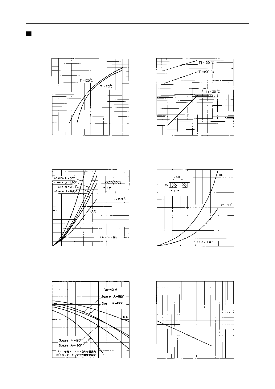
Forward characteristics
V
F
[V]
I
F
[A]
Reverse characteristics
V
R
[V]
I
R
[mA]
Reverse power dissipation
W
R
[
W
]
V
R
[V]
T
c
[
įC
]
I
o
[
A
]
Output current-case temperature
W
F
[
W
]
I
o
[A]
Forward power dissipation
Junction capacitance characteristics
C
j
[pF]
V
R
[V]
0 5 10 15
5 10 30 50 100
50
30
10
5
3
1
0 0.2 0.4 0.6 0.8 1.0 1.2
10
1
0.1
0.01
20
16
12
8
4
0
0 10 20 30 40 50
0 10 20 30 40 50 60 70
7.5
5.0
2.5
0
0 2 4 6 8 10 12 14 16 18 20
3000
1000
500
300
100
140
120
100
80
60
