MS808C06
(30A)
(60V / 30A )
Features
Low V
F
Super high speed switching
High reliability by planer design
Applications
High speed power switching
Maximum ratings and characteristics
Absolute maximum ratings
Item
Repetitive peak reverse voltage
Non-repetitive peak reverse voltage
Average output current
Surge current
Operating junction temperature
Storage temperature
Symbol
V
RRM
V
RSM
I
o
I
FSM
T
j
T
stg
Conditions
Sine wave
10ms
200
-40 to +150
-40 to +150
Unit
V
V
A
A
∞C
∞C
Electrical characteristics (Ta=25∞C Unless otherwise specified )
Item
Forward voltage drop
Reverse current
Thermal resistance
Symbol
V
FM
I
RRM
R
th(j-c)
Conditions
I
FM
=12.5A
V
R
=V
RRM
Junction to case
Max.
0.58
20
1.2
Unit
V
mA
∞C/W
tw=500ns, duty=
1/40
Square wave, duty=
1/2
Tc=118∞C
Rating
60
60
30*
SCHOTTKY BARRIER DIODE
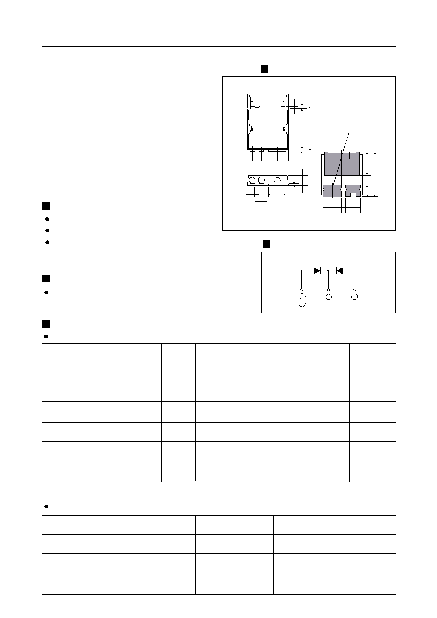
Outline drawings, mm
Connection diagram
1
3
2
*
Average forward current of centertap full wave connection
4
(4.0)
(3.2)
(2.2)
(2.1)
(10.1)
(5.8)
Solder
Plating
10.1
±0.3
9.0
±0.2
0.5
±0.2
2.8
±0.2
0.4
±0.1
3.6
±0.2
1.0
±0.2
1.0
±0.2
9.0
±0.2
7.0
±0.2
2.0
2.0 2.5
1.5
3
1
2
4
0.1
(0.8)
0.6
±0.2

TS808C06 (30A)
(60V / 30A )
Characteristics
0.01
0.1
1
10
100
0.0
0.1
0.2
0.3
0.4
0.5
0.6
0.7
0.8
0.9
1.0
Tj=150
o
C
Tj=125
o
C
Tj=100
o
C
Tj=25
o
C
Forward Characteristic
(typ.)
IF Forward Current (A)
VF Forward Voltage (V)
0
10
20
30
40
50
60
70
10
-3
10
-2
10
-1
10
0
10
1
10
2
Reverse Characteristic (typ.)
Tj= 25
o
C
Tj=100
o
C
Tj=125
o
C
Tj=150
o
C
IR Reverse Current (mA)
VR Reverse Voltage (V)
0
2
4
6
8
10
12
14
16
0
2
4
6
8
10
12
14
16
18
20
22
Per 1element
DC
Square wave
=180
o
Sine wave
=180
o
Square wave
=120
o
Square wave
=60
o
Forward Power Dissipation
WF Forward Power Dissipation (W)
Io Average Forward Current (A)
0
10
20
30
40
50
60
70
0
2
4
6
8
10
12
14
16
18
20
Reverse Power Dissipation
=180
o
DC
PR Reverse Power Dissipation (W)
Reverse Voltage
0
5
10
15
20
25
30
35
40
45
60
70
80
90
100
110
120
130
140
150
160
:Conduction angle of forward current for each rectifier element
Io:Output current of center-tap full wave connection
Square wave
=120
o
Square wave
=60
o
Square wave
=180
o
Sine wave
=180
o
DC
Current Derating (Io-Tc)
Tc Case Temperature (
o
C )
Io Average Output Current (A)
360∞
Io
360∞
VR
VR=30V
360∞
Io
10
100
100
1000
Junction Capacitance Characteristic (typ.)
Cj Junction Capacitance (pF)
VR Reverse Voltage (V)

TS808C06 (30A)
(60V / 30A )
1
10
100
10
100
1000
Surge Capability
I FSM Peak Half - Wave Current (A)
Number of Cycles at 50Hz
10
-3
10
-2
10
-1
10
0
10
1
10
2
10
-2
10
-1
10
0
10
1
Transient Thermal Impedance
Transient Thermal Impedance (
o
C/W )
t Time (sec.)