
MS906C3
(20A)
(300V / 20A )
Features
Low V
F
Low height : 2.8mm
Small mounting area
High reverse voltage
Center tap connection
Applications
High frequency operation
DC-DC converters
AC adapter
Maximum ratings and characteristics
Absolute maximum ratings
Item
Repetitive peak reverse voltage
Repetitive peak surge reverse voltage
Average output current
Surge current
Operating junction temperature
Storage temperature
Symbol
V
RRM
V
RSM
I
o
I
FSM
T
j
T
stg
Conditions
Sine wave
10ms
-40 to +150
Unit
V
V
A
A
∞C
∞C
Electrical characteristics (Tc=25∞C Unless otherwise specified )
Item
Forward voltage drop
Reverse current
Reverse recovery time
Symbol
V
FM
I
RRM
trr
Conditions
I
FM
=10A
V
R
=V
RRM
IF=0.1A, IR=0.2A,
Irec=0.05A
Max.
1.2
200
35
Unit
V
µ
A
ns
Square wave, duty=
1/2
Tc=95∞C
Rating
300
300
20
80
+150
Low loss fast recovery diode
Outline drawings, mm
Connection diagram
(4.0)
(3.2)
(2.2)
(2.1)
(10.1)
(5.8)
Solder
Plating
10.1
±0.3
9.0
±0.2
0.5
±0.2
2.8
±0.2
0.4
±0.1
3.6
±0.2
1.0
±0.2
1.0
±0.2
9.0
±0.2
7.0
±0.2
2.0
2.0 2.5
1.5
3
1
2
4
0.1
(0.8)
0.6
±0.2
1
3
2
4
Electrical characteristics (Tc=25∞C Unless otherwise specified )
Major characteristics
Characteristics
MS906C3
Units Condition
V
RRM
300
V
V
F
0.89
V
Tj=125∞C, typ
I
O
20
A
Item
Thermal resistance
Symbol
Rth(j-c)
Condition
Junction to case
Max.
2
Unit
∞C/W
*
Average output current at centertap full wave connection
*
tw=500ns, duty=1/40
MS906C3 (20A)
Characteristics
(300V / 20A )
0.01
0.1
1
10
100
0.0
0.2
0.4
0.6
0.8
1.0
1.2
1.4
Tj=25∞C
Tj=100∞C
Tj=125∞C
Tj=150∞C
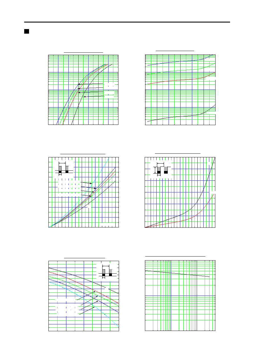
Forward Characteristic (typ.)
IF Forward Current (A)
VF Forward Voltage (V)
0
50
100
150
200
250
300
10
-3
10
-2
10
-1
10
0
10
1
Tj=25∞C
Tj=100∞C
Tj=125∞C
Reverse Characteristic (typ.)
Tj=150∞C
IR Reverse Current (mA)
VR Reverse Voltage (V)
0
1
2
3
4
5
6
7
8
9
10
0
2
4
6
8
10
12
14
Square wave
=60∞
Square wave
=120∞
Sine wave
=180∞
Square wave
=180∞
Per 1element
DC
Forward Power Dissipation
WF Forward Power Dissipation (W)
Io Average Forward Current (A)
0
25
50
75 100 125 150 175 200 225 250 275 300
0
1
2
3
4
5
6
=180
o
Reverse Power Dissipation
DC
PR Reverse Power Dissipation (W)
VR Reverse Voltage (V)
0
5
10
15
20
60
70
80
90
100
110
120
130
140
150
160
Sine wave
=180∞
Square wave
=180∞
Square wave
=120∞
Square wave
=60∞
:Conduction angle of forward current for each rectifier element
Io:Output current of center-tap full wave connection
DC
Current Derating (Io-Tc)
Tc Case Temperature (∞C)
Io Average Output Current (A)
360∞
Io
360∞
Io
360∞
V
R
1
10
100
1
10
100
Junction Capacitance Characteristic (typ.)
CJ Junction Capacitance (pF)
VR Reverse Voltage (V)

MS906C3 (20A)
(300V / 20A )
1
10
100
10
100
1000
Surge Capability
IFSM Peak Half - Wave Current (A)
Number of Cycles at 50Hz
10
-3
10
-2
10
-1
10
0
10
1
10
2
10
-1
10
0
10
1
10
2
Transient Thermal Impedance
Transient Thermal Impedance (∞C/W)
t Time (s)