 | –≠–ª–µ–∫—Ç—Ä–æ–Ω–Ω—ã–π –∫–æ–º–ø–æ–Ω–µ–Ω—Ç: MB47393 | –°–∫–∞—á–∞—Ç—å:  PDF PDF  ZIP ZIP |

DS04-12103-4E
FUJITSU SEMICONDUCTOR
DATA SHEET
ASSP
DUAL COMPARATOR
MB47393
s
DESCRIPTION
The Fujitsu MB47393 is a dual comparator which is designed to operate from a single power supply over a wide
range of voltage. The input characteristics is equivalent of current industry standard comparator. Even though
operated from a single power supply, the input common mode voltage range includes ground. Owing to adoption
of clamp circuitry in input pins, mis-operation is prevented by negative input. The MB47393 is compatible with
LM393.
s
FEATURES
∑ Wide power supply voltage range
Single power supply ≠≠≠ 2V to 30V
Dual power supplies ≠≠≠ ±1V to ±15V
∑ Wide input common-mode voltage range
0V to (V
CC
≠ 1.5)V
∑ Low input bias current ≠≠≠ 25nA typ.
∑ High sink current capability because of open collector output 40mA min.
∑ Package
Plastic 8 pin DIP package
(Suffix: ≠P)
Plastic 8 pin FPT package
(Suffix: ≠PF)
Plastic 9 pin SIP package
(Suffix: ≠PS)
s
PACKAGE
PLAPMSTIC PACKAGE
DIP-08P-M01
PLAPMSTIC PACKAGE
FPT-08P-M01
PLAPMSTIC PACKAGE
SIP-09P-M01

2
MB47393
s
PIN ASSIGNMENT
s
ABSOLUTE MAXIMUM RATINGS (see NOTE)
Ta = 25∞C
* : This value is specified with respect to the short circuit from output to GND. However, short circuit from the output
to V
CC
cause device destruction.
Note: Permanent device damage may occur if the above Absolute Maximum Ratings are exceeded. Functional
operation should be restricted to the conditions as detailed in the operational sections of this data sheet.
Exposure to absolute maximum rating conditions for extended periods may affect device reliability.
Rating
Symbol
Value
Unit
Power Supply Voltage
V
CC
36
V
Differential Input Voltage
V
ID
36
V
Common-Mode Input Voltage
V
I
≠5 to +36
V
Output Short Current to GND
≠≠
Infinite*
≠≠
Power Dissipation
P
D
350 (Ta
55∞C)
mW
Operating Temperature
Ta
≠20 to +75
∞C
Storage Temperature
T
STG
≠55 to +125
∞C
+ ≠
+ ≠
+ ≠
≠ +
OUT A
1
2
3
4
≠ IN A
+ IN A
GND
8
7
6
5
V
CC
OUT B
≠ IN B
+ IN B
(TOP VIEW)
(DIP-8P-M01)
(FPT-8P-M01)
(TOP VIEW)
(SIP-9P-M01)
9
8
7
6
5
4
3
2
1
V
CC
OUT B
≠ IN B
OUT A
GND
+ IN A
≠ IN A
V
CC
+ IN B

3
MB47393
s
RECOMMENDED OPERATING CONDITIONS
Parameter
Symbol
Value
Unit
Power Supply Voltage
V
CC
2 to 30
V
±1.0 to ±15
Operating Temperature
Ta
≠20 to +75
∞C
Output Sink Current
I
SINK
40
mA
Figure 1 MB47393 EQUIVALENT CIRCUIT
OUT
V
CC
1k
≠ IN
+ IN
1k

4
MB47393
s
ELECTRICAL CHARACTERISTICS
(
Ta = 25∞C, V
CC
= 5V)
Notes:
*1: I
IN
is measured when V
I
S 0 and direction of the input current flows from IC. When negative voltage is applied
to input pin, the pin is equivalently connected the GND through a 1k
of resistor.
When low voltage below than ≠5V is applied, please connect a resistor serially to input pin in order to prevent
the high current flow.
*2: Positive input voltage may exceed the power supply voltage. As long as the other voltage remains in the common-
mode input voltage range, the comparator will provide a proper output state.
When V
CC
= 5V, your are requested to use V
IN
below 25V.
s
TYPICAL CHARACTERISTIC CURVES
Parameter
Symbol
Condition
Value
Unit
Min.
Typ.
Max.
Input Offset Voltage
V
IO
V
O
= V
REF
= 1.4V
≠≠
2
5
mV
Input Offset Current
I
IO
≠≠
≠≠
5
50
nA
Input Bias Current
I
IN*1
≠≠
≠≠
25
250
nA
Common-Mode Input Voltage
V
CM*2
≠≠
0
≠≠
V
CC
≠1.5
V
Power Supply Current
I
CC
R
L
=
≠≠
2
3
mA
Voltage Gain
A
V
R
L
= 15k
, V
CC
= 15V
≠≠
200
≠≠
V/mV
Response Time
≠≠
R
L
= 1k
≠≠
2
≠≠
µs
Output Sink Current
I
SINK
V
IN(+)
= 0, V
IN(≠)
= 1V, V
OL
1.5V
40
≠≠
≠≠
mA
Output Saturation Voltage
V
OL
V
IN(+)
= 0, V
IN(≠)
= 1V, I
SINK
= 30mA
≠≠
0.2
0.4
V
Output Leakage Current
I
LEAK
V
IN(+)
= 1V, V
IN(≠)
= 0V, V
O
= 30V
≠≠
≠≠
1
µA
Figure 2 POWER SUPPLY CURRENT
vs POWER SUPPLY VOLTAGE
Figure 3 OUTPUT SATURATION VOLTAGE
vs OUTPUT SINK CURRENT
PO
WE
R
SUPPL
Y CURRENT I
CC
(m
A)
O
U
TPUT
SA
T
U
RA
TION V
O
L
T
A
G
E V
O
L
(V)
TA = ≠30∞C
25∞C
75∞C
40
20
30
10
40
30
20
10
0
TA = 75∞C
10
1
0.1
0.01
0.001
25∞C
≠30∞C
5
MB47393
s
TYPICAL CHARACTERISTIC CURVES (Continued)
INP
U
T V
O
L
T
A
G
E
V
IN
(m
V)
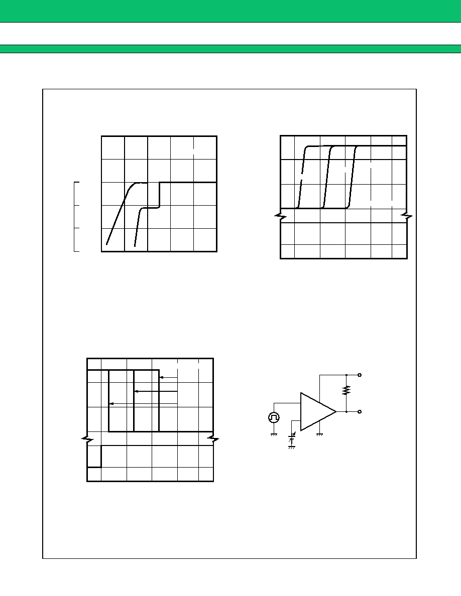
Figure 4 INPUT CURRENT
vs INPUT VOLTAGE
Figure 5 INPUT VOLTAGE/OUTPUT
VOLTAGE vs RESPONSE TIME
Figure 6 INPUT VOLTAGE/OUTPUT
VOLTAGE vs RESPONSE TIME
Figure 7 TEST CIRCUIT
(µA)
≠300
≠100
0
100
50
0
≠50
≠100
≠150
(nA)
I
N
P
U
T CURR
E
N
T I
IN
≠
INPUT VOLTAGE V
IN≠
(V)
≠1.0
≠0.5
0
10
20
30
V
CC
= 5V
TIME t (µs)
OU
TP
U
T
V
O
L
T
A
G
E
V
O
(V)
6
Input Over Drive
5mV
20mV
4
2
0
100
0
0
0.5
1
1.5
2
IN
P
U
T
V
O
L
T
A
G
E
V
IN
(mV
)
TIME t (µs)
OUTP
UT V
O
L
T
A
G
E
V
O
(V
)
6
Input Over Drive
5mV
4
2
0
0
≠100
0
0.5
1
1.5
2
20mV
100mV
100mV
≠
+
V
CC =
5V
V
O
V
REF
PG
R
L
= 5.1k
Over drive value is fixed by V
REF
.