 | –≠–ª–µ–∫—Ç—Ä–æ–Ω–Ω—ã–π –∫–æ–º–ø–æ–Ω–µ–Ω—Ç: MB86064 | –°–∫–∞—á–∞—Ç—å:  PDF PDF  ZIP ZIP |

MB86064
Copyright © 2004 Fujitsu Microelectronics Europe GmbH
Production
Page 1 of 4
Disclaimer: The contents of this document are subject to change without notice. Customers are advised to consult with FUJITSU sales representatives before
ordering.The information and circuit diagrams in this document are presented "as is", no license is granted by implication or otherwise.
Product Flyer
October 2004
Version 1.1
FME/MS/DAC80/FL/5085
Dual 14-bit 1GSa/s DAC
Mixed Signal Division
The Fujitsu MB86064 is a Dual 14-bit 1GSa/s digital to analog
converter (DAC), delivering exceptional dynamic performance.
Each high performance DAC core is capable of generating
multi-standard, multi-carrier communication transmit signals,
suitable for 2, 2.5 and 3G systems. DAC data is input via two
high-speed LVDS ports. These operate in a pseudo double data
rate (DDR) mode, with data latched on both rising and falling
edges. Alternatively, the device can be configured as a
multiplexed dual-port single DAC. To simplify system
integration the DAC operates from a clock running at half the
DAC conversion rate.
Features
∑ Dual 14-bit, 1GSa/s Digital to Analog conversion
∑ Exceptional dynamic performance
∑
74dBc ACLR for 4 UMTS carriers @ 276MHz direct-IF
∑ 100MHz image-free generated bandwidth capability
∑
supports UMTS plus digital pre-distortion bandwidth
∑ Proprietary performance enhancement features
∑ LVDS data interface
∑ Register selectable on-chip LVDS termination resistors
∑ Fujitsu 4-wire serial control interface
∑ Two 16k point programmable on-chip waveform memories
∑ Low power 3.3V analog and 1.8V digital operation
∑ 750mW per DAC power dissipation at 1GSa/s
∑ 0.18µm CMOS technology with Triple Well
∑ Performance enhanced EFBGA package
∑ Industrial temperature range (-40∞C to +85∞C)
Applications
∑ Multi-carrier, Multi-standard cellular infrastructure
∑
CDMA, W-CDMA, GSM/EDGE, UMTS
∑ Wideband communications systems
∑ High Direct-IF architectures
∑ Arbitrary waveform generation
∑ Test equipment
∑ Radar, video & display systems
PLASTIC PACKAGE
EFBGA-120
Package Dimensions
12 mm x 12 mm
PIN ASSIGNMENT
Not to scale. Viewed from above.
E3
E1
F4
F2
G3
G1
H4
H2
J3
J1
K4
K2
L3
L1
M4
M2
N3
N1
P4
P2
R3
R1
T4
T2
U3
V2
W3
W1
AA5
AC5
Y6
AB6
AA7
AC7
Y8
AB8
AA9
AC9
Y10
AB10
AA11
AC11
Y12
AB12
AA13
AC13
Y14
AB14
AA15
AC15
Y16
AB16
AA17
AC17
Y18
AB18
AA19
AC19
W21
W23
V20
V22
U21
U23
T20
T22
R21
R23
P20
P22
N21
N23
M20
M22
L21
L23
K20
K22
J21
J23
H20
H22
G21
G23
F20
F22
E21
E23
C19
A19
D18
B18
C17
A17
B16
D16
A15
C15
B14
D14
A13
C13
B12
D12
A11
C11
B10
D10
A9
C9
B8
A7
C7
D8
B6
D6
A5
C5
Index
N10
N12
N14
R10
R12
R14
L10
L12
L14
J10
J12
J14
K9
K11
K13
K15
M9
M11
M13
M15
P9
P11
P13
P15
SER
I
A
L
_
I
N
SER
I
A
L
_
E
N
AVS
S
IO
U
T
B
_
B
IO
U
T
_
B
AV
D
3
3
BG
A
P
A
V
D
18
_C
L
K
AV
D
2
5
AV
D
3
3
IO
U
T
_
A
IO
U
T
B
_
A
AVS
S
DA
C_
S
C
A
N
SP
AR
E
CL
K
I
N
CL
K
I
NB
VL
O
W
_
A
A
V
D
18
_A
A
V
D
18
_A
X_
R
E
SET
T
EST
VL
O
W
_
B
X_A10
VR
EF
RR
E
F
AVS
S
SER
I
A
L
_
O
U
T
SER
I
A
L
_
C
L
K
A
V
D
18
_B
A
V
D
18
_B
A10
DVSS
DVDD
DVDD
DVSS
A8
A6
X_A8
X_A6
A2
X_A2
A4
DVDD
X_B9
DVSS
X_A4
B9
X_B10
B10
DVDD
DVSS
DVDD
DVSS
DVDD
DVSS
X_A3
A3
A1
NC
X_A1
DVSS
NC
A5
X_A5
A7
X_A7
DVDD
A9
X_A9
B1
3
X_
B
1
3
DV
S
S
LP
C
L
K
_
OU
T
A1
3
X_
L
P
C
L
K
_
I
N
LP
C
L
K
_
I
N
X_
L
P
C
L
K
_
O
U
T
X_
A
1
3
DV
S
S
X_
A
1
1
A1
1
CL
K
1
_
O
UT
A1
4
DV
DD
X_
A1
2
X
_
CL
K
1
_
O
UT
X_
A1
4
A1
2
B1
1
DV
S
S
X_
B1
4
X_
C
L
K2
_
O
U
T
CL
K
2
_
O
UT
DV
DD
X_
B1
2
DV
DD
B1
4
B1
2
X_
B
1
1
B6
X_B6
B8
X_B8
B2
X_B2
X_B3
B1
B3
DVDD
X_B4
B5
NC
X_B1
DVSS
B4
X_B5
B7
X_B7
NC
U1
V4
All centre pins : TG
October 2004 Version 1.1
FME/MS/DAC80/FL/5085
MB86064 Dual 14-bit 1GSa/s DAC
Page 2 of 4
Production
Copyright © 2004 Fujitsu Microelectronics Europe GmbH
Disclaimer: The contents of this document are subject to change without notice. Customers are advised to consult with FUJITSU sales representatives before
ordering.The information and circuit diagrams in this document are presented "as is", no license is granted by implication or otherwise.
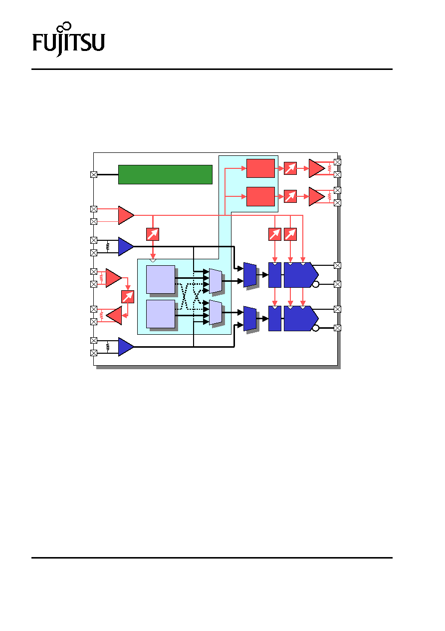
Functional Overview
The MB86064 is a high performance Dual 14-bit 1GSa/s DAC. In addition to two DAC cores the
device features a host of features designed to help both system integration and operation. A
functional block diagram is shown in Figure 1. Analog performance at high frequencies is enhanced
by novel current switch and switch driver designs which provide constant data-independent switching
delay, reducing jitter and distortion.
Figure 1 MB86064 Functional Block Diagram
The device requires an input clock at half the DAC conversion rate as each DAC core is clocked on
both edges of the input clock. Each DAC core can be regarded as two interleaved DACs, each
running at half rate. The main reason for adopting this approach is that the switch driver inherently
includes a multiplex function through its two input ports. Compared to a conventional switch driver
this allows twice as long to acquire and convert, though because the two paths share current sources
they match exactly at low frequencies. A characteristic of this architecture is a suppressed image
appearing reflected about Fs(dac)/4 of Fclk-Fsig. Duty cycle error in the input clock will exacerbate
this image, but can be minimised by trimming the differential DC offset at the clock input pins.
The big advantage of this approach compared to a single DAC running at half the rate is much
reduced sinx/x roll off, which gives increased output power and better in-band flatness when
generating high output frequencies (e.g. 200MHz and above). This is illustrated in Figure 2 as line 1.
An alternative approach using a return-to-zero output stage has the same sinx/x roll off (and switch
driver speed) but 6dB lower output power and a large image at Fclk-Fout. See Line 2.
Port A data input
14-bit LVDS
Port B data input
14-bit LVDS
Waveform
Memory
A
(16K Points)
Waveform
Memory
A
(16K Points)
W
a
v
e
fo
rm
Mem
o
r
y
Mo
du
le
Waveform
Memory
B
(16K Points)
Waveform
Memory
B
(16K Points)
RF Clock input
e.g. 500MHz
Loop clock input
LVDS
Loop clock output
LVDS
Clock output 2
LVDS
Clock output 1
LVDS
4-wire Serial Control Interface
Control Interface
1.8V LVCMOS
Analog output A
Analog output B
EFBGA-120
˜
˜
˜
˜
1, 2, 4, 8
DAC A
(14-bit)
DAC B
(14-bit)
˜
˜
˜
˜
1, 2, 4, 8
Double-Edge
clocked
(1GSa/s)

October 2004 Version 1.1
FME/MS/DAC80/FL/5085
MB86064 Dual 14-bit 1GSa/s DAC
Copyright © 2004 Fujitsu Microelectronics Europe GmbH
Production
Page 3 of 4
Disclaimer: The contents of this document are subject to change without notice. Customers are advised to consult with FUJITSU sales representatives before
ordering.The information and circuit diagrams in this document are presented "as is", no license is granted by implication or otherwise.
Line 3 illustrates a conventional DAC
running at half rate.
Input Data
Unsigned binary data to each DAC core is
input via a dedicated parallel LVDS port. As
with the DAC core, data is latched on every
rising and falling edge of the clock in a
pseudo DDR mode. For synchronisation of
data generator(s) two LVDS clock outputs
and a Loop-Clock facility are provided.
Loop-Clock
Maintaining valid clock-to-data timing becomes increasingly difficult at higher clock rates, particularly
taking into account device-to-device variations. The MB86064 minimises potential problems through
its DDR data interface and by providing a loop-clock facility. The on-chip `loop' consists of an LVDS
input connected to an LVDS output, through a programmable delay stage. This loop-through, and the
associated tracking from the data generating device, should be incorporated in the feedback loop of
a Delay-Locked Loop (DLL) or Phase-Locked Loop (PLL) clock generator, within the data generating
device. This enables the system to compensate for variations in input/output delays in both the data
generating device and the DAC.
Performance Enhancement Features
Each DAC core integrates a number of performance enhancing features. Performance levels now
reach the level sought after for next generation systems and high direct-IF architectures.
Serial Control Interface
A Fujitsu 4-wire serial interface is provided for configuration and control of the DAC. Programmed
data is stored in a number of read/writable registers.
Waveform Memory Module
The MB86064 incorporates a Waveform Memory Module featuring two 16k point on-chip waveform
memories. These allow the DAC cores to be driven with user programmed waveforms without the
need for external high speed, pattern generators.
Development Kit
A comprehensive Development Kit (DK),
DK86064, is available which comprises a
number of modules. A base motherboard
provides an interface to the DAC, Clock and
Data modules. Also included is a PC USB
Interface Lead & Control Software.
For further details, please refer to the
associated documentation.
0
dBFS
Frequency
-6
Target high direct-IF
generating region
Figure 2 Benefits of DAC core architecture to
Sinx/x response

4
Worldwide Headquarters
Japan
Asia
Tel: +81 44 754 3753
Fax: +81 44 754 3329
Fujitsu Limited
Kamikodanaka 4-1-1
Nakahara-ku
Kawasaki-shi
Kanagawa-ken 211-8588
Japan
Tel: +65 281 0770
Fax: +65 281 0220
Fujitsu Microelectronics Asia Pte Ltd
151 Lorong Chauan
New Tech Park
#05-08
Singapore 556741
http://www.fujitsu.com
http://www.fmal.fujitsu.com
USA
Europe
Tel: +1 408 737 5600
Fax: +1 408 737 5999
Fujitsu Microelectronics America, Inc.
1250 E. Arques Avenue, M/S 333
Sunnyvale, CA 94088-3470
USA
T
el: +49 6103 6900
Fax: +49 6103 690122
Fujitsu Microelectronics Europe GmbH
Am Siebenstein 6-10
D-63303 Dreieich-Buchschlag
Germany
Tel: +1 800 866 8608
Fax: +1 408 737 5984
Customer Response Center
Mon-Fri: 7am-5pm (PST)
http://www.fma.fujitsu.com/
http://www.fme.fujitsu.com/
October 2004
Version
1.1
FME/MS/DAC80/FL/5085
MB86064 Dual 14-bit 1GSa/s DAC
Page 4 of 4
Production
Copyright © 2004 Fujitsu Microelectronics Europe GmbH
Disclaimer: The contents of this document are subject to change without notice. Customers are advised to consult with FUJITSU sales representatives before
ordering.The information and circuit diagrams in this document are presented "as is", no license is granted by implication or otherwise.
FME/MS/DAC80/FL/5085 1.1
The contents of this document are subject to change without notice. Customers are advised to consult with FUJITSU sales
representatives before ordering.
The information and circuit diagrams in this document presented as examples of semiconductor device applications, and are not
intended to be incorporated in devices for actual use. Also, FUJITSU is unable to assume responsibility for infringement of any patent
rights or other rights of third parties arising from the use of this information or circuit diagrams. No license is granted by implication
or otherwise under any patent or patent rights of Fujitsu Microelectronics Europe GmbH.
FUJITSU semiconductor devices are intended for use in standard applications (computers, office automation and other office
equipment, industrial, communications, and measurement equipment, personal or household devices, etc.).
CAUTION: Customers considering the use of our products in special applications where failure or abnormal operation may directly
affect human lives or cause physical injury or property damage, or where extremely high levels of reliability are demanded (such as
aerospace systems, atomic energy controls, sea floor repeaters, vehicle operating controls, medical devices for life support, etc.)
are requested to consult with FUJITSU sales representatives before such use. The company will not be responsible for damages
arising from such use without prior approval.
Any semiconductor devices have inherently a certain rate of failure. You must protect against injury, damage or loss from such
failures by incorporating safety design measures into your facility and equipment such as redundancy, fire protection, and prevention
of over-current levels and other abnormal operating conditions.
If any products described in this document represent goods or technologies subject to certain restrictions on export under the Foreign
Exchange and Foreign Trade Control Law of Japan, the prior authorization by Japanese government should be required for export
of those products from Japan.