FEATURES
MECHANICAL DATA
Case: TO-92 Plastic Package
Weight: approx. 0.18 g
MAXIMUM RATINGS AND ELECTRICAL CHARACTERISTICS
Small Signal Transistors (NPN)
B
E
C
.181 (4.6)
mi
n. .492
(
12.5)
.181 (
4
.6)
.142 (3.6)
Dimensions in inches and (millimeters)
TO-92
Ratings at 25 ∞C
ambient temperature unless otherwise specified
.098 (2.5)
max.
.022 (0.55)
4/98
BC546 THRU BC549
Symbol
Value
Unit
Collector-Base Voltage
BC546
BC547
BC548, BC549
V
CBO
V
CBO
V
CBO
80
50
30
V
V
V
Collector-Emitter Voltage
BC546
BC547
BC548, BC549
V
CES
V
CES
V
CES
80
50
30
V
V
V
Collector-Emitter Voltage
BC546
BC547
BC548, BC549
V
CEO
V
CEO
V
CEO
65
45
30
V
V
V
Emitter-Base Voltage
BC546, BC547
BC548, BC549
V
EBO
V
EBO
6
5
V
V
Collector Current
I
C
100
mA
Peak Collector Current
I
CM
200
mA
Peak Base Current
I
BM
200
mA
Peak Emitter Current
≠I
EM
200
mA
Power Dissipation at T
amb
= 25 ∞C
P
tot
500
1)
mW
Junction Temperature
T
j
150
∞C
Storage Temperature Range
T
S
≠65 to +150
∞C
1)
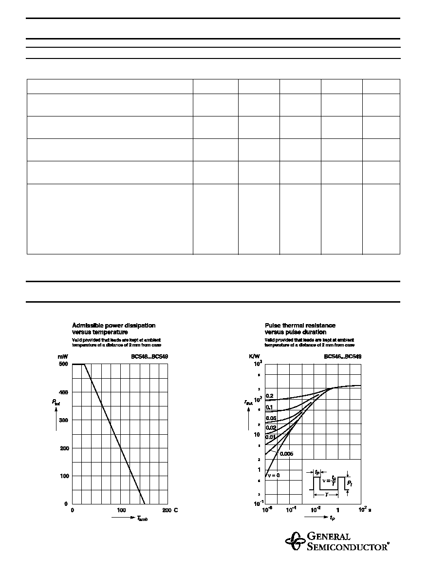
Valid provided that leads are kept at ambient temperature at a distance of 2 mm from case
NPN Silicon Epitaxial Planar Transistors
These transistors are subdivided into three groups
A, B and C according to their current gain. The type
BC546 is available in groups A and B, how-
ever, the types BC547 and BC548 can be
supplied in all three groups. The BC549 is a
low-noise type and available in groups B and
C. As complementary types, the PNP transis-
tors BC556 ... BC559 are recommended.
On special request, these transistors are also
manufactured in the pin configuration TO-18.

ELECTRICAL CHARACTERISTICS
Ratings at 25 ∞C
ambient temperature unless otherwise specified
Symbol
Min.
Typ.
Max.
Unit
h-Parameters at V
CE
= 5 V, I
C
= 2 mA,
f = 1 kHz,
Small Signal Current Gain
Current Gain Group A
B
C
Input Impedance
Current Gain Group A
B
C
Output Admittance
Current Gain Group A
B
C
Reverse Voltage Transfer Ratio
Current Gain Group A
B
C
h
fe
h
fe
h
fe
h
ie
h
ie
h
ie
h
oe
h
oe
h
oe
h
re
h
re
h
re
≠
≠
≠
1.6
3.2
6
≠
≠
≠
≠
≠
≠
220
330
600
2.7
4.5
8.7
18
30
60
1.5 ∑ 10
≠4
2 ∑ 10
≠4
3 ∑ 10
≠4
≠
≠
≠
4.5
8.5
15
30
60
110
≠
≠
≠
≠
≠
≠
k
k
k
µ
S
µ
S
µ
S
≠
≠
≠
DC Current Gain
at V
CE
= 5 V, I
C
= 10
µ
A
Current Gain Group A
B
C
at V
CE
= 5 V, I
C
= 2
mA
Current Gain Group A
B
C
at V
CE
= 5 V, I
C
= 100 mA
Current Gain Group A
B
C
h
FE
h
FE
h
FE
h
FE
h
FE
h
FE
h
FE
h
FE
h
FE
≠
≠
≠
110
200
420
≠
≠
≠
90
150
270
180
290
500
120
200
400
≠
≠
≠
220
450
800
≠
≠
≠
≠
≠
≠
≠
≠
≠
≠
≠
≠
Thermal Resistance Junction to Ambient Air
R
thJA
≠
≠
250
1)
K/W
Collector Saturation Voltage
at I
C
= 10 mA, I
B
= 0.5 mA
at I
C
= 100 mA, I
B
= 5 mA
V
CEsat
V
CEsat
≠
≠
80
200
200
600
mV
mV
Base Saturation Voltage
at I
C
= 10 mA, I
B
= 0.5 mA
at I
C
= 100 mA, I
B
= 5 mA
V
BEsat
V
BEsat
≠
≠
700
900
≠
≠
mV
mV
Base-Emitter Voltage
at V
CE
= 5 V, I
C
= 2 mA
at V
CE
= 5 V, I
C
= 10 mA
V
BE
V
BE
580
≠
660
≠
700
720
mV
mV
Collector-Emitter Cutoff Current
at V
CE
= 80 V
BC546
at V
CE
= 50 V
BC547
at V
CE
= 30 V
BC548, BC549
at V
CE
= 80 V, T
j
= 125 ∞C
BC546
at V
CE
= 50 V, T
j
= 125 ∞C
BC547
I
CES
I
CES
I
CES
I
CES
I
CES
≠
≠
≠
≠
≠
0.2
0.2
0.2
≠
≠
15
15
15
4
4
nA
nA
nA
µ
A
µ
A
1)
Valid provided that leads are kept at ambient temperature at a distance of 2 mm from case
BC546 THRU BC549
ELECTRICAL CHARACTERISTICS
Ratings at 25 ∞C
ambient temperature unless otherwise specified
Symbol
Min.
Typ.
Max.
Unit
at V
CE
= 30 V, T
j
= 125 ∞C
BC548, BC549
I
CES
≠
≠
4
4
µ
A
µ
A
Gain-Bandwidth Product
at V
CE
= 5 V, I
C
= 10 mA, f = 100 MHz
f
T
≠
300
≠
MHz
Collector-Base Capacitance
at V
CB
= 10 V, f = 1 MHz
C
CBO
≠
3.5
6
pF
Emitter-Base Capacitance
at V
EB
= 0.5 V, f = 1 MHz
C
EBO
≠
9
≠
pF
Noise Figure
at V
CE
= 5 V, I
C
= 200
µ
A, R
G
= 2 k
,
f = 1 kHz,
f = 200 Hz
BC546, BC547
BC548
BC549
at V
CE
= 5 V, I
C
= 200
µ
A, R
G
= 2 k
,
f = 30...15000 Hz
BC549
F
F
F
≠
≠
≠
2
1.2
1.4
10
4
4
dB
dB
dB
BC546 THRU BC549
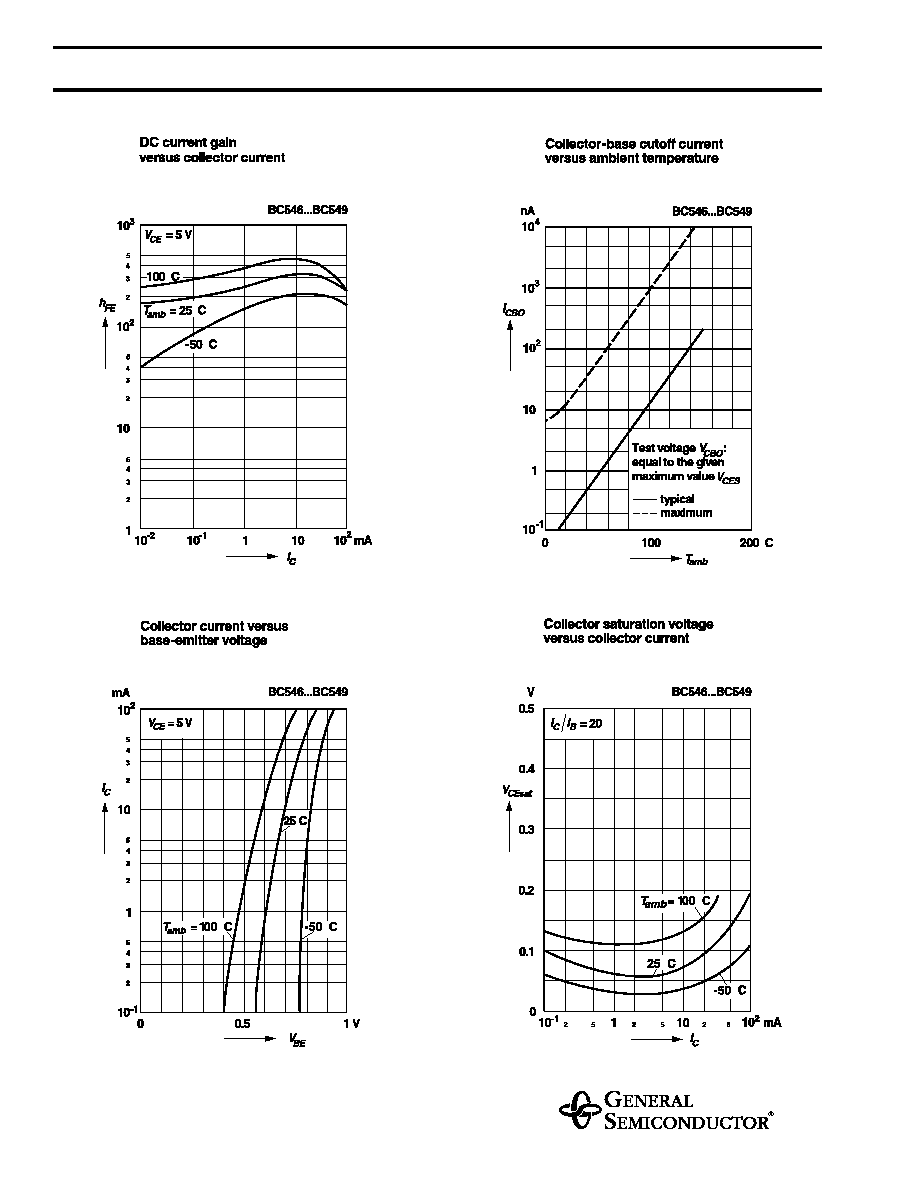
RATINGS AND CHARACTERISTIC CURVES BC546 THRU BC549