 | –≠–ª–µ–∫—Ç—Ä–æ–Ω–Ω—ã–π –∫–æ–º–ø–æ–Ω–µ–Ω—Ç: MMBT3906 | –°–∫–∞—á–∞—Ç—å:  PDF PDF  ZIP ZIP |
MMBT3906
SMALL SIGNAL TRANSISTORS (PNP)
FEATURES
® PNP Silicon Epitaxial Planar Transistor
for switching and amplifier applications.
® As complementary type, the NPN
transistor MMBT3904 is recommended.
® This transistor is also available in the TO-92 case with
the type designation 2N3906.
MECHANICAL DATA
Case: SOT-23 Plastic Package
Weight: approx. 0.008g
Marking code: 2A
MAXIMUM RATINGS AND ELECTRICAL CHARACTERISTICS
Ratings at 25°C ambient temperature unless otherwise specified
SYMBOL
VALUE
UNIT
Collector-Base Voltage
–V
CBO
40
V
Collector-Emitter Voltage
–V
CEO
40
V
Emitter-Base Voltage
–V
EBO
5.0
V
Collector Current
–I
C
200
mA
Power Dissipation at T
A
= 25 °C
P
tot
225
(1)
mW
300
(2)
mW
Thermal Resistance Junction to Substrate Backside
R
qSB
320
(1)
°C/W
Thermal Resistance Junction to Ambient Air
R
qJA
450
(1)
°C/W
Junction Temperature
T
j
150
°C
Storage Temperature Range
T
S
–55 to +150
°C
NOTES:
(1) Device on fiberglass subtrate, see layout
(2) Device on alumina substrate
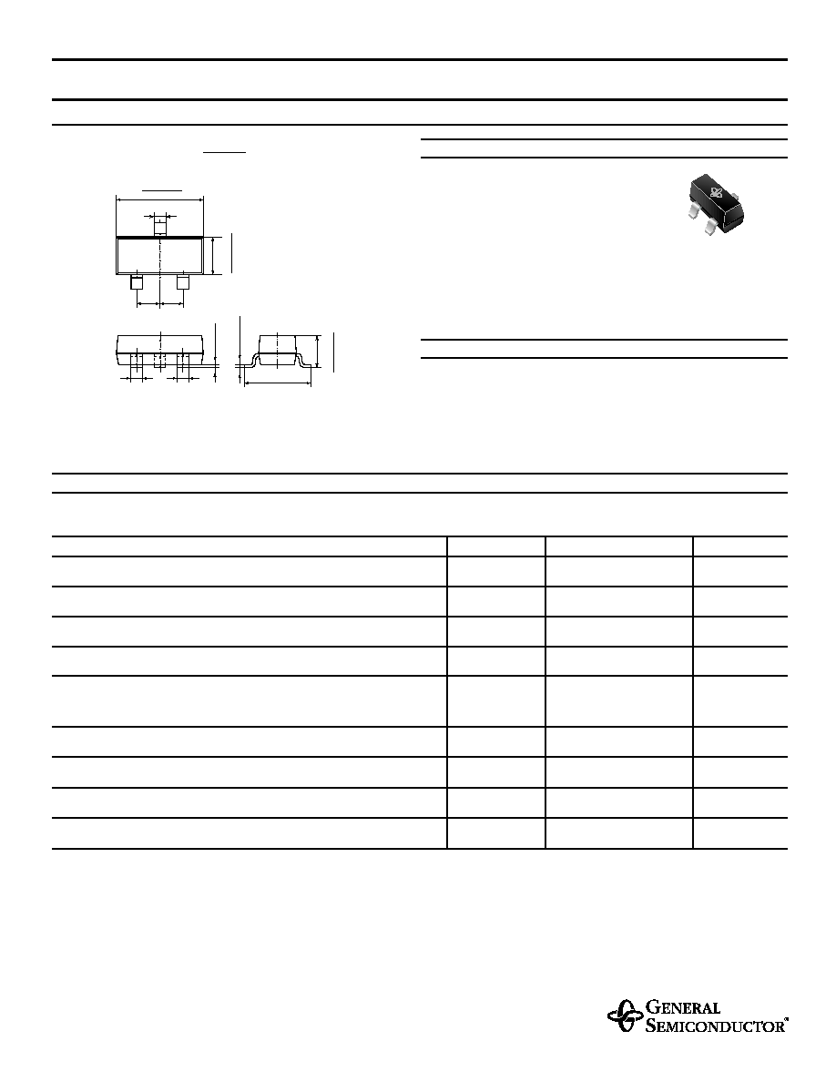
.016 (0.4)
.056 (
1
.43
)
.037(0.95) .037(0.95)
ma
x
.
.004
(
0.1
)
.122 (3.1)
.016 (0.4)
.016 (0.4)
1
2
3
Top View
.102 (2.6)
.007 (
0
.17
5)
.0
45 (
1
.15)
.118 (3.0)
.052 (
1
.33
)
.005
(
0
.1
25)
.094 (2.4)
.0
37 (
0
.95)
SOT-23
1/5/99
Dimensions in inches and (millimeters)
Pin configuration
1 = Base, 2 = Emitter, 3 = Collector.
NEW PRODUCT
NEW PRODUCT
NEW PRODUCT

MMBT3906
ELECTRICAL CHARACTERISTICS
Ratings at 25°C ambient temperature unless otherwise specified
SYMBOL
MIN.
MAX.
UNIT
Collector-Base Breakdown Voltage
at –I
C
= 10
mA, I
E
= 0
–V
(BR)CBO
40
–
V
Collector-Emitter Breakdown Voltage
at –I
C
= 1 mA, I
B
= 0
–V
(BR)CEO
40
–
V
Emitter-Base Breakdown Voltage
at –I
E
= 10
mA, I
C
= 0
–V
(BR)EBO
5
–
V
Collector Saturation Voltage
at –I
C
= 10 mA, –I
B
= 1 mA
–V
CEsat
–
0.25
V
at –I
C
= 50 mA, –I
B
= 5 mA
–V
CEsat
–
0.4
V
Base Saturation Voltage
at –I
C
= 10 mA, –IB = 1 mA
–V
BEsat
–
0.85
V
at –I
C
= 50 mA, –IB = 5 mA
–V
BEsat
–
0.95
V
Collector-Emitter Cutoff Current
at –V
EB
= 3 V, –V
CE
= 30 V
–I
CEV
–
50
nA
Emitter-Base Cutoff Current
at –V
EB
= 3 V, –V
CE
= 30 V
–I
EBV
–
50
nA
DC Current Gain
at –V
CE
= 1 V, –I
C
= 0.1 mA
h
FE
60
–
–
at –V
CE
= 1 V, –I
C
= 1 mA
h
FE
80
–
–
at –V
CE
= 1 V, –I
C
= 10 mA
h
FE
100
300
–
at –V
CE
= 1 V, –I
C
= 50 mA
h
FE
60
–
–
at –V
CE
= 1 V, –I
C
= 100 mA
h
FE
30
–
–
Input Impedance
at –V
CE
= 10 V, –I
C
= 1 mA, f = 1 kHz
h
ie
1
10
k
W
Gain-Bandwidth Product
at –V
CE
= 20 V, –I
C
= 10 mA, f = 100 MHz
f
T
250
–
MHz
Collector-Base Capacitance
at –V
CB
= 5 V, f = 100 kHz
C
CBO
–
4.5
pF
Emitter-Base Capacitance
at –V
EB
= 0.5 V, f = 100 kHz
C
EBO
–
10
pF
MMBT3906
ELECTRICAL CHARACTERISTICS
Ratings at 25°C ambient temperature unless otherwise specified
SYMBOL
MIN.
MAX.
UNIT
Voltage Feedback Ratio
at –V
CE
= 10 V, –IC = 1 mA, f = 1 kHz
h
re
0.5 · 10
–4
8 · 10
–4
–
Small Signal Current Gain
at –V
CE
= 10 V, –IC = 1 mA, f = 1 kHz
h
fe
100
400
–
Output Admittance
at –V
CE
= 1 V, –I
C
= 1 mA, f = 1 kHz
h
oe
1
40
mS
Noise Figure
at –V
CE
= 5 V, –I
C
= 100
mA, R
G
= 1 k
W,
f = 10 … 15 000 Hz
NF
–
4
dB
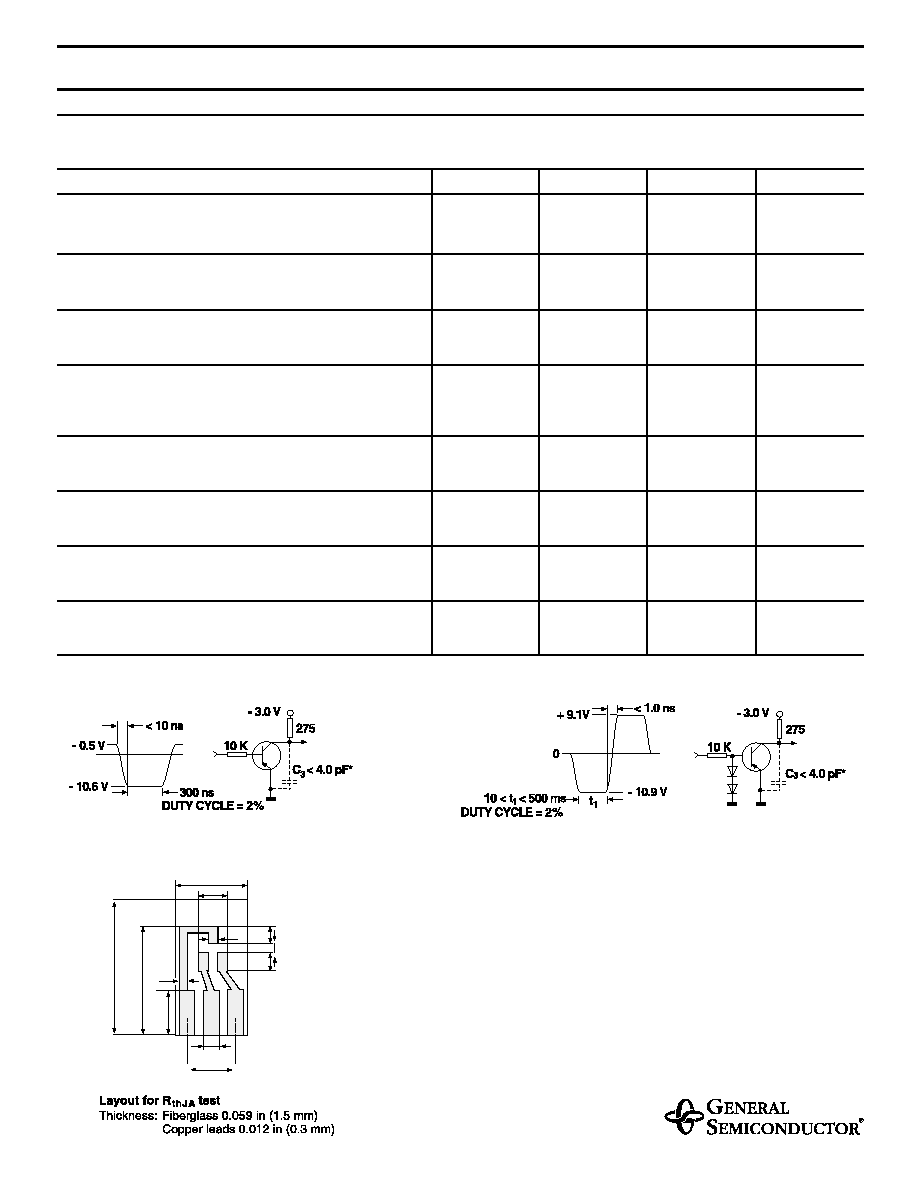
Delay Time (see Fig. 1)
at –I
B1
= 1 mA, –I
C
= 10 mA
t
d
–
35
ns
Rise Time (see Fig. 1)
at –I
B1
= 1 mA, –I
C
= 10 mA
t
r
–
35
ns
Storage Time (see Fig. 2)
at I
B1
= –I
B2
= 1 mA, –I
C
= 10 mA
t
s
–
225
ns
Fall Time (see Fig. 2)
at I
B1
= –I
B2
= 1 mA, –I
C
= 10 mA
t
f
–
75
ns
Fig. 2: Test circuit for storage and fall time
* total shunt capacitance of test jig and connectors
Fig. 1: Test circuit for delay and rise time
* total shunt capacitance of test jig and connectors
0.59 (15)
0.2 (5)
0.03 (0.8)
0.30 (7.5)
0.12 (3)
.04 (1)
0.06 (1.5)
0.20 (5.1)
.08 (2)
.08 (2)
.04 (1)
0.47 (12)
Dimensions in inches and (millimeters)