SMAJ5.0 THRU SMAJ170CA
SURFACE MOUNT T
RANS
Z
ORB
TM TRANSIENT VOLTAGE SUPPRESSOR
Stand-off Voltage - 5.0 to 170 Volts Peak Pulse Power - 300 Watts
FEATURES
Optimized for LAN protection applications
Ideal for ESD protection of data lines in accordance
with IEC 1000-4-2 (IEC801-2)
Ideal for EFT protection of data lines in accordance with
IEC1000-4-4 (IEC801-4)
Plastic package has Underwriters Laboratory
Flammability Classification 94V-0
Glass passivated junction
Excellent clamping capability
Low incremental surge resistance
Fast response time: typically less than 1.0ps from 0 Volts
to V
(BR)
min.
300W peak pulse power capability with a 10/1000
µ
s
waveform, repetition rate (duty cycle): 0.01%
High temperature soldering guaranteed:
250∞C/10 seconds at terminals
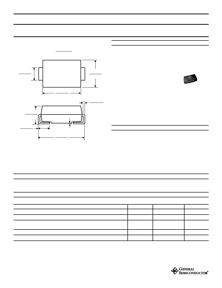
MECHANICAL DATA
Case: JEDEC DO-214AC molded plastic body over
passivated chip
Terminals: Solder plated, solderable per MIL-STD-750,
Method 2026
Polarity: For uni-directional types the color band denotes
the cathode, which is postitive with respect to the anode
under normal TVS operation
Mounting Position: Any
Weight: 0.002 ounces, 0.064 gram
DEVICES FOR BIDIRECTIONAL APPLICATIONS
For bi-directional use suffix C or CA for types SMAJ5.0 thru SMAJ170 (e.g. SMAJ5.0C, SMAJ170CA)
Electrical characteristics apply in both directions.
MAXIMUM RATINGS AND ELECTRICAL CHARACTERISTICS
Ratings at 25∞C ambient temperature unless otherwise specified.
SYMBOLS
VALUE
UNITS
Peak pulse power dissipation with a 10/1000
µ
s waveform
(NOTE 1, 2, FIG.1)
P
PM
Minimum 300
Watts
Peak pulse current with a 10/1000
µ
s waveform
(NOTE 1)
I
PPM
SEE TABLE 1
Amps
Peak forward surge current 8.3ms single half sine-wave superimposed
on rated load (JEDEC Method)
(NOTES 2, 3)
- unidirectional only
I
FSM
40.0
Amps
Maximum instantaneous forward voltage at 25A
(NOTE 3)
V
F
3.5
Volts
Operating junction and storage temperature range
T
J
, T
STG
-55 to +150
∞C
NOTES:
(1) Non-repetitive current pulse, per Fig.3 and derated above T
A
=25∞C per Fig. 2
(2) Mounted on 0.2 x 0.2" (5.0 x 5.0mm) copper pads to each terminal
(3) Measured on 8.3ms single half sine-wave. For uni-directional devices only.
1/20/99
0.157 (3.99)
0.177 (4.50)
0.006 (0.152)
0.012 (0.305)
0.030 (0.76)
0.060 (1.52)
0.008 (0.203) MAX.
0.194 (4.93)
0.208 (5.28)
0.100 (2.54)
0.110 (2.79)
0.078 (1.98)
0.090 (2.29)
0.049 (1.25)
0.065 (1.65)
DO-214AC
Dimensions in inches and (millimeters)

RECOMMENDED PAD LAYOUT
The pad dimensions should be 0.010" (2.5mm) longer than the contact size in the lead
axis. This allows a solder fillet to form, see figure below. Contact factory for soldering
methods.
MODIFIED J-BEND
0.060 MIN
(1.52 MIN)
0.050 MIN
(1.27 MIN)
0.220 REF
(5.58)
0.094 MAX
(2.38 MAX)
Dimensions in inches and (millimeters)
ELECTRICAL CHARACTERISTICS (T
A
=25∞C unless otherwise noted) TABLE 1 (Cont'd)
Device
Marking Code
Device
UNI
BI
SMAJ54
RD
ZD
60.0
73.3
1.0
54
5.0
96.3
3.1
SMAJ54A
RE
ZE
60.0
66.3
1.0
54
5.0
87.1
3.4
SMAJ58
RF
ZF
64.4
78.7
1.0
58
5.0
103
2.9
SMAJ58A
RG
ZG
64.4
71.2
1.0
58
5.0
93.6
3.2
SMAJ60
RH
ZH
66.7
81.5
1.0
60
5.0
107
2.8
SMAJ60A
RK
ZK
66.7
73.7
1.0
60
5.0
96.8
3.1
SMAJ64
RL
ZL
71.1
86.4
1.0
64
5.0
114
2.6
SMAJ64A
RM
ZM
71.1
78.6
1.0
64
5.0
103
2.9
SMAJ70
RN
ZN
77.8
95.1
1.0
70
5.0
125
2.4
SMAJ70A
RP
ZP
77.8
86
1.0
70
5.0
113
2.7
SMAJ75
RQ
ZQ
83.3
102
1.0
75
5.0
134
2.2
SMAJ75A
RR
ZR
83.3
92.1
1.0
75
5.0
121
2.5
SMAJ78
RS
ZS
86.7
106
1.0
78
5.0
139
2.2
SMAJ78A
RT
ZT
86.7
95.8
1.0
78
5.0
126
2.4
SMAJ85
RU
ZU
94.4
115
1.0
85
5.0
151
2
SMAJ85A
RV
ZV
94.4
104
1.0
85
5.0
137
2.2
SMAJ90
RW
ZW
100
122
1.0
90
5.0
160
1.9
SMAJ90A
RX
ZX
100
111
1.0
90
5.0
146
2.1
SMAJ100
RY
ZY
111
136
1.0
100
5.0
179
1.7
SMAJ100A
RZ
ZZ
111
123
1.0
100
5.0
162
1.9
SMAJ110
SD
VD
122
149
1.0
110
5.0
196
1.5
SMAJ110A
SE
VE
122
135
1.0
110
5.0
177
1.7
SMAJ120
SF
VF
133
163
1.0
120
5.0
214
1.4
SMAJ120A
SG
VG
133
147
1.0
120
5.0
193
1.6
SMAJ130
SH
VH
144
176
1.0
130
5.0
231
1.3
SMAJ130A
SK
VK
144
159
1.0
130
5.0
209
1.4
SMAJ150
SL
VL
167
204
1.0
150
5.0
268
1.1
SMAJ150A
SM
VM
167
185
1.0
150
5.0
243
1.2
SMAJ160
SN
VN
178
218
1.0
160
5.0
287
1.0
SMAJ160A
SP
VP
178
197
1.0
160
5.0
259
1.2
SMAJ170
SQ
VQ
189
231
1
170
5.0
304
0.99
SMAJ170A
SR
VR
189
209
1.0
170
5.0
275
1.09
This device is designed specifically for transient voltage suppression from
threats generated by ESD for board level load switching components.
The wide leads assure a large surface contact for good heat dissipation,
and a low resistance path for surge current flow to ground.
This series is designed to optimize board space and for use with surface
mount technology automated assembly equipment.
They can be easily mounted on printed circuit boards and ceramic
substrates to protect sensitive components from transient voltage
damage.
APPLICATION NOTES
Test
Current
I
T
(mA)
Working Peak
Reverse Voltage
V
WM
(Volts)
Breakdown Voltage
V
(BR)
(Volts) at I
T
(NOTE 1)
Min.
Max.
Maximum Clamping
Voltage at I
PPM
Vc (Volts)
Maximum
Peak Pulse
Surge Current I
PPM
(NOTE 2)
(Amps)
Maximum
Reverse
Leakage
a V
WM
(NOTE 3)
I
D (
µ
A)
NOTES:
(1) V
(BR)
measured after I
T
applied for 300
µ
s square wave pulse or equivalent
(2) Surge current waveform per Fig. 3 and derate per Fig. 2
(3) For bi-directional types having V
WM
of 10 Volts and less, the I
D
limit is doubled
(4) For the bi-directional SMAJ5.0CA, the maximum V
(BR)
is 7.25V.
(5) All terms and symbols are consistent with ANSI/IEEE C62.35
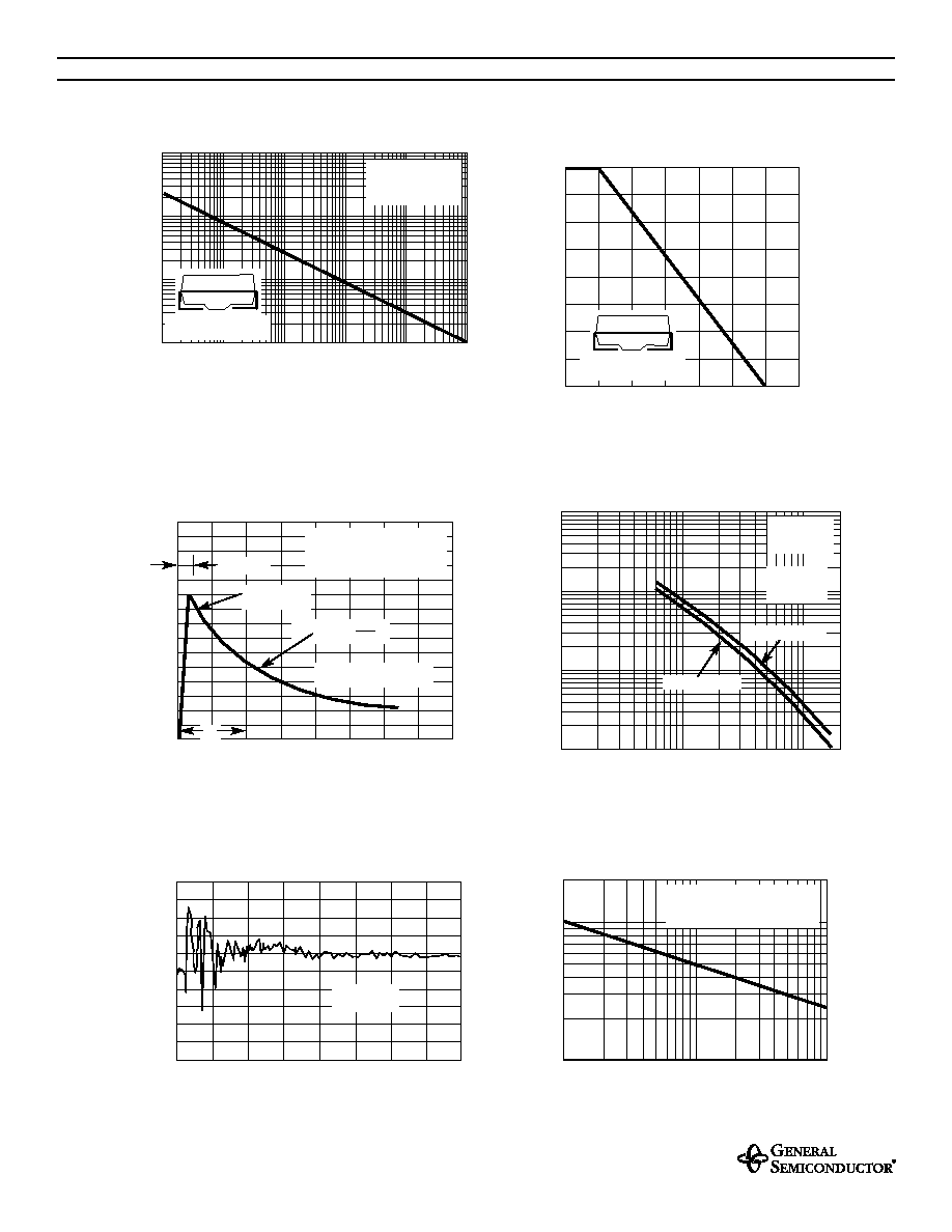
0
1.0
2.0
3.0
4.0
0
100
150
50
1
10
100
0
10
20
30
40
50
0.1
m
s
1.0
m
s
10
m
s
100
m
s
1.0ms
10ms
0.1
1.0
10
100
0
50
100
150
0
25
50
75
100
25
75
125
175
1
10
100
200
10
100
1,000
10,000
MAXIMUM RATINGS AND CHARACTERISTIC CURVES SMAJ5.0 THRU SMAJ170CA
105
84
63
42
21
0V
-21
-42
-63
-84
-105
0
10
20
30
40
50
60
70
FIG. 5- Typical Response to 8KV Positive Going ESD Pulse
Per IEC1000 - 4-2 (IEC801-2)
t, TIME, nsec
LET
THROUGH VOL
T
AGE, VOL
TS
FIG. 1 - PEAK PULSE POWER RATING CURVE
P
PPM
, PEAK PULSE POWER, kW
td, PULSE WIDTH, sec.
T
A
, AMBIENT TEMPERATURE, ∞C
FIG. 4 - TYPICAL JUNCTION CAPACITANCE
FIG. 3 - PULSE WAVEFORM
t, TIME, ms
V
(BR)
, BREAKDOWN VOLTAGE, VOLTS
NUMBER OF CYCLES AT 60 H
Z
I
PPM,
PEAK PULSE CURRENT
, %
PEAK PULSE POWER (Ppp) or CURRENT
(
IPPM
)
DERA
TING IN PERCENT
AGE, %
C
J,
JUNCTION CAP
ACIT
ANCE, pF
I
FSM
, PEAK FOR
W
ARD SURGE CURRENT
,
AMPERES
NON-REPETITIVE
PULSE WAVEFORM
SHOWN in FIG. 3
T
A
=25∞C
PULSE WIDTH (td) is DEFINED
as the POINT WHERE the PEAK
CURRENT DECAYS
to 50% of I
PPM
tr=10
µ
sec.
T
J
=25∞C
f=1.0 MH
Z
Vsig=50mVp-p
Measured at
Stand-off
Voltage, V
WM
UNI-DIRECTIONAL
BI-DIRECTIONAL
Device Used:
SMAJ15C
T
J
=T
J
max.
8.3ms SINGLE HALF SINE-WAVE
(JEDEC Method)
td
PEAK VALUE
I
PPM
HALF VALUE - I
PPM
2
10/1000
µ
sec. WAVEFORM
as DEFINED by R.E.A.
FIG. 6 - MAXIMUM NON-REPETITIVE FORWARD SURGE
CURRENT UNIDIRECTIONAL ONLY
FIG. 2 - PULSE DERATING CURVE
0.2 x 0.2" (5.0 x 5.0mm)
COPPER PAD AREAS
0.2 x 0.2" (5.0 x 5.0mm)
COPPER PAD AREAS