SS32 thru SS36
Vishay Semiconductors
formerly General Semiconductor
Document Number 88751
www.vishay.com
1-Jul-02
1
Surface Mount Schottky Rectifier
Reverse Voltage 20 to 60V
Forward Current 3.0A
Mounting Pad Layout
Maximum Ratings and Thermal Characteristics
(T
A
= 25∞C unless otherwise noted)
Parameter
Symbol
SS32
SS33
SS34
SS35
SS36
Unit
Device marking code
S2
S3
S4
S5
S6
Maximum repetitive peak reverse voltage
V
RRM
20
30
40
50
60
V
Maximum RMS voltage
V
RMS
14
21
28
35
42
V
Maximum DC blocking voltage
V
DC
20
30
40
50
60
V
Maximum average forward rectified current at T
L
(See Fig. 1)
I
F(AV)
3.0
A
Peak forward surge current 8.3ms single half sine-
wave superimposed on rated load (JEDEC Method)
I
FSM
100
A
Typical thermal resistance
(2)
R
JA
55
R
JL
17
∞C/W
Operating junction temperature range
T
J
≠55 to +125
≠55 to +150
∞C
Storage temperature range
T
STG
≠55 to +150
∞C
Electrical Characteristics
(T
A
= 25∞C unless otherwise noted)
Maximum instantaneous forward voltage at 3.0A
(1)
V
F
0.50
0.75
V
Maximum DC reverse current
T
A
=25∞C
0.5
at rated DC blocking voltage
(1)
T
A
=100∞C
I
R
20
10
mA
Notes: (1) Pulse test: 300
µ
s pulse width, 1% duty cycle
(2) P.C.B. mounted 0.55 x 0.55" (14 x 14mm) copper pad areas
Features
∑ Plastic package has Underwriters Laboratory
Flammability Classification 94V-0
∑ Low profile surface mount package
∑ Built-in strain relief
∑ Low power loss, high efficiency
∑ For use in low voltage high frequency inverters,
free wheeling, and polarity protection applications
∑ Guardring for overvoltage protection
∑ High temperature soldering guaranteed:
250∞C/10 seconds at terminals
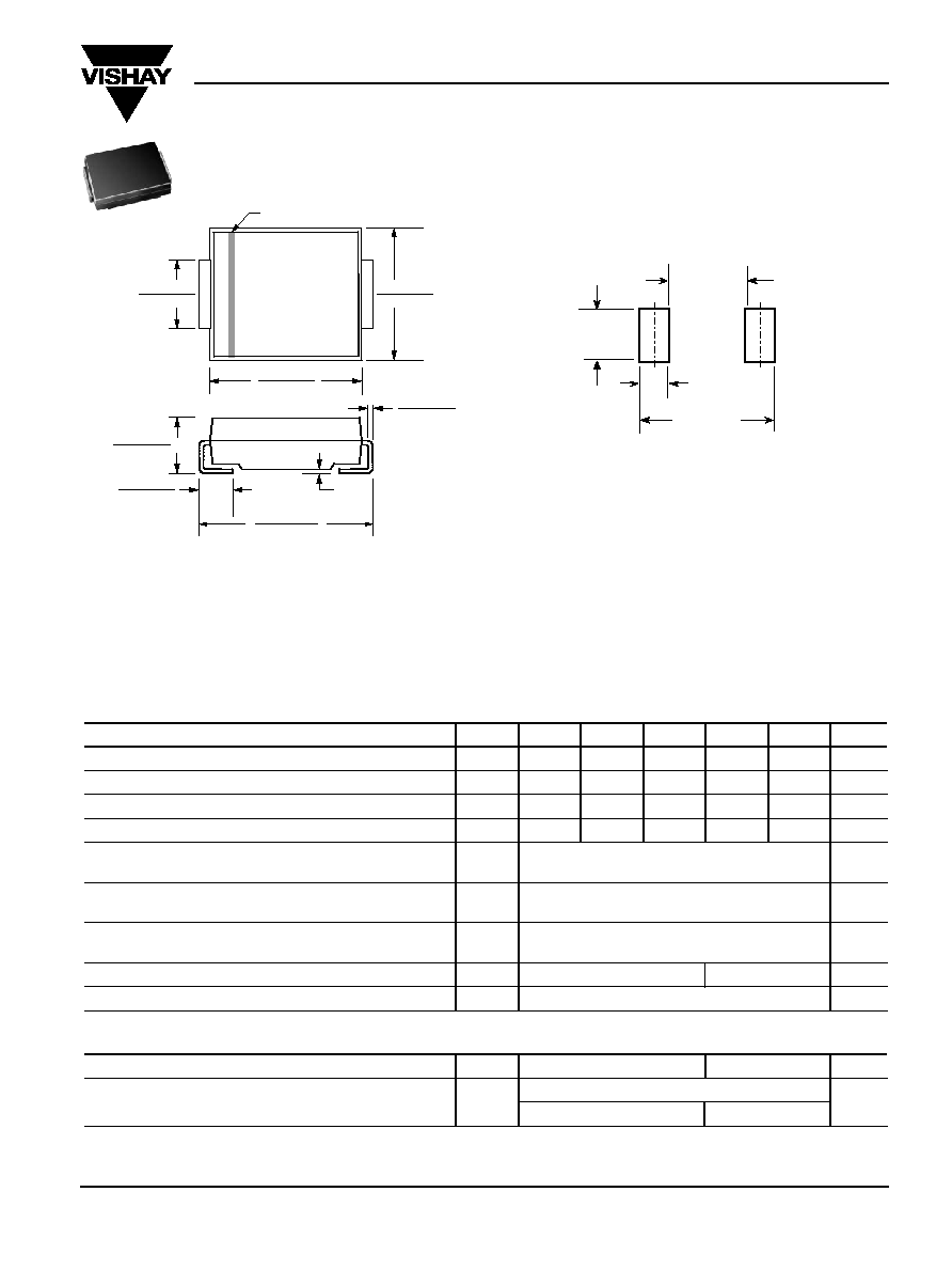
Mechanical Data
Case: JEDEC DO-214AB molded plastic body
Terminals: Solder plated, solderable per
MIL-STD750, Method 2026
Polarity: Color band denotes cathode end
Weight: 0.007 oz., 0.25 g
0.185 MAX.
(4.69 MAX.)
0.121 MIN.
(3.07 MIN.)
0.060 MIN.
(1.52 MIN.)
0.320 REF
0.280 (7.11)
0.260 (6.60)
0.012 (0.305)
0.006 (0.152)
0.008
(0.203)
Max.
0.320 (8.13)
0.305 (7.75)
0.060 (1.52)
0.030 (0.76)
0.245 (6.22)
0.220 (5.59)
0.126 (3.20)
0.114 (2.90)
0.103 (2.62)
0.079 (2.06)
Cathode Band
Dimensions in inches
and (millimeters)
DO-214AB (SMC)

50
70
90
110
130
150
0
1.0
2.0
3.0
1
10
100
0
20
40
60
80
100
0
20
40
60
80
100
0.001
0.01
0.1
1
10
20
0.1
1
10
100
10
100
1,000
0
0.4
0.8
1.2
0.01
0.1
1
10.0
30.0
0.2
0.6
1.0
1.4
1.6
0.01
0.1
1
10.0
100
0.1
1
10.0
100
P.C.B. Mounted on
0.55 x 0.55" (14 x 14mm)
Copper Pad Areas
Resistive or Inductive Load
SS32 - SS34
SS35 & SS36
SS32 - SS34
SS35 & SS36
SS32 - SS34
SS35 & SS36
SS32 - SS34
SS35 & SS36
At rated T
L
8.3ms single half sine-wave
(JEDEC Method)
Pulse width = 300
µ
s
1% Duty Cycle
T
J
= 125
∞
C
T
J
= 25
∞
C
T
J
= 150
∞
C
T
A
= 125
∞
C
T
A
= 75
∞
C
T
A
= 25
∞
C
T
J
= 25
∞
C
f = 1.0 MHz
Vsig = 50mVp-p
Fig. 1 - Forward Current
Derating Curve
Fig. 3 - Typical Instantaneous
Forward Characteristics
Fig. 5 - Typical Junction
Capacitance
Fig. 2 - Maximum Non-repetitive
Peak Forward Surge Current
Fig. 4 - Typical Reverse Current
Characteristics
Fig. 6 - Maximum Non-repetitive
Peak Forward Surge Current
Average Forward Current (A)
Peak Forward Surge Current (A)
Lead Temperature (
∞
C)
Instantaneous Forwad Current (A)
Instantaneous Forward Voltage (V)
Junction Capacitance (pF)
Reverse Voltage (V)
Transient Thermal Impedance (
∞
C/W)
t, Pulse Duration (sec.)
Instantaneous Reverse Current (mA)
Percent of Rated Peak Reverse Voltage (%)
Number of Cycles at 60Hz
SS32 thru SS36
Vishay Semiconductors
formerly General Semiconductor
www.vishay.com
Document Number 88751
2
1-Jul-02
Ratings and
Characteristic Curves
(T
A
= 25∞C unless otherwise noted)