 | –≠–ª–µ–∫—Ç—Ä–æ–Ω–Ω—ã–π –∫–æ–º–ø–æ–Ω–µ–Ω—Ç: G692 | –°–∫–∞—á–∞—Ç—å:  PDF PDF  ZIP ZIP |
Ver: 1.0
Sep 23, 2002
TEL: 886-3-5788833
http://www.gmt.com.tw
1
G692/G693
Global Mixed-mode Technology Inc.
4-Pin µP Voltage Monitors with Manual Reset Input
Features
Precision Monitoring of +3V, +3.3V, and +5V
Power-Supply Voltages
Fully Specified Over Temperature
Available in Three Output Configurations
Push-Pull RESET Output (G692L)
Push-Pull RESET Output (G692H)
Open-Drain RESET Output (G693L)
140ms min Power-On Reset Pulse Width
5µA Supply Current
Guaranteed Reset Valid to V
CC
= +1V
Power Supply Transient Immunity
No External Components
Manual Reset Input
4-Pin SOT143 Package
Applications
Computers
Controllers
Intelligent Instruments
Critical µP and µC Power Monitoring
Portable / Battery-Powered Equipment
Automotive
General Description
The G692/G693 are microprocessor (µP) supervisory
circuits used to monitor the power supplies in µP and
digital systems. They provide excellent circuit reliability
and low cost by eliminating external components and
adjustments when used with +5V, +3.3V, +3.0V- pow-
ered circuits. The G692/G693 also provide a de-
bounced manual reset input.
These circuits perform a single function: they assert a
reset signal whenever the V
CC
supply voltage declines
below a preset threshold, keeping it asserted for at
least 140ms after V
CC
has risen above the reset
threshold. Reset thresholds suitable for operation with
a variety of supply voltages are available.
The G693L has an open-drain output stage, while the
G692 have push-pull outputs. The G693L's open-drain
RESET output requires a pull-up resistor that can be
connected to a voltage higher than V
CC
. The G692L
have an active-low RESET output, while the G692H
has an active-high RESET output. The reset com-
parator is designed to ignore fast transients on V
CC
,
and the outputs are guaranteed to be in the correct
logic state for V
CC
down to 1V.
Low supply current makes the G692/G693 ideal for
use in portable equipment. The G692/G693 are avail-
able in a 4-pin SOT143 packages.
Ordering Information
PART TEMP.
RANGE PIN-PACKAGE
G692H(L)xxxTC -40∞C ~ +105∞C SOT143
G693LxxxTC
-40∞C ~ +105∞C
SOT143
* xxx specifies the threshold voltage.
e.g. 263 denotes the 2.63V threshold voltage.
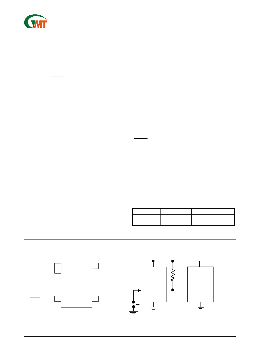
Pin Configuration Typical Operating Circuit
RESET
INPUT
GND
µP
V
CC
RESET
(RESET)
GND
G692/G693
V
CC
R
PULL-UP
V
CC
*
*G693 ONLY
MR
V
CC
SOT143
G692/G693
4
GND
2
RESET(RESET)
MR
3
()is for G692H
1
RESET
INPUT
GND
µP
V
CC
RESET
(RESET)
GND
G692/G693
V
CC
R
PULL-UP
V
CC
*
*G693 ONLY
MR
RESET
INPUT
GND
µP
V
CC
RESET
(RESET)
GND
G692/G693
V
CC
R
PULL-UP
V
CC
*
*G693 ONLY
MR
V
CC
SOT143
G692/G693
4
GND
2
RESET(RESET)
MR
3
()is for G692H
1
V
CC
SOT143
G692/G693
4
GND
2
RESET(RESET)
MR
3
()is for G692H
1

Ver: 1.0
Sep 23, 2002
TEL: 886-3-5788833
http://www.gmt.com.tw
2
G692/G693
Global Mixed-mode Technology Inc.
Absolute Maximum Ratings
Terminal Voltage (with respect to GND)
V
CC
..................................................-0.3V to +6.0V
RESET, RESET (push-pull)...........-0.3V to (V
CC
+ 0.3V)
RESET (open drain).............................-0.3V to +6.0V
Input Current, V
CC
................................................20mA
Output Current, RESET, RESET ........................20mA
Continuous Power Dissipation (T
A
= +70∞C)
SOT 143 (derate 4mW/∞C above +70∞C)...........320mW
Operating Temperature Range ............-40∞C to +105∞C
Storage Temperature Range................-65∞C to +150∞C
Lead Temperature (soldering, 10s) ...................+300∞C
Stresses beyond those listed under "Absolute Maximum Ratings" may cause p'ermanent damage to the device. These are stress rat-
ings only, and functional operation of the device at these or any other conditions beyond those indicated in the operational sections of
the specifications is not implied. Exposure to absolute maximum rating conditions for extended periods may affect device reliability.
Electrical Characteristics
(V
CC
= full range, T
A
= -40∞C to +105∞C, unless otherwise noted. Typical values are at T
A
= +25∞C, V
CC
= 5V
for 463/438/400 versions, V
CC
= 3.3V for 308/293 versions, and V
CC
= 3V for 263 version.) (Note 1)
PARAMETER SYMBOL
CONDITION
MIN
TYP
MAX
UNITS
T
A
= 0∞C +70∞C
1.0
5.5
V
CC
Range
T
A
= -40∞C +105∞C
1.2
5.5
V
V
CC
<5.5V, G69_ _463/438/400_
5.5
9
Supply Current
I
CC
T
A
= -40∞C +105∞C
V
CC
<3.6V, G69_ _308/293/263_
5
8
µA
G69_ _463_
T
A
= +25∞C
4.537 4.63 4.722
G69_ _438_
T
A
= +25∞C
4.292 4.38 4.467
G69_ _400_
T
A
= +25∞C
3.92 4.00
4.08
G69_ _308_
T
A
= +25∞C
3.018 3.08 3.141
G69_ _293_
T
A
= +25∞C
2.871 2.93 2.988
Reset Threshold
V
TH
G69_ _263_
T
A
= +25∞C
2.577 2.63 2.682
V
Ver: 1.0
Sep 23, 2002
TEL: 886-3-5788833
http://www.gmt.com.tw
3
G692/G693
Global Mixed-mode Technology Inc.
Electrical Characteristics
(Continued)
(V
CC
= full range, T
A
= -40∞C to +105∞C, unless otherwise noted. Typical values are at T
A
= +25∞C, V
CC
= 5V
for 463/438/400 versions, V
CC
= 3.3V for 308/293 versions, and V
CC
= 3V for 263 version.) (Note 1)
PARAMETER SYMBOL
CONDITION
MIN
TYP
MAX
UNITS
Reset Threshold Tempco
70
ppm/∞C
V
CC
to Reset Delay (Note 2)
V
CC
= V
TH
to (V
TH
≠ 100mV)
15
V
CC
= V
TH
max, G69_ _ 463/438/400
250
510
720
Reset Active Timeout Period
V
CC
= V
TH
max, G69_ _308/293/263
140
310
520
ms
MR
Minima Pulse Width
t
MR
10
µs
MR
Glitch Immunity (Note 3)
100
ns
MR
to Reset Propagation Delay
(Note 2)
t
MD
0.5
µs
V
IH
0.6 x V
CC
MR
Input Threshold
V
IL
V
CC
> V
TH(max)
0.25 x V
CC
V
MR
Pull-up Resistance
10 20 30 K
RESET
Output Current Low
(push-pull active low, and open-
drain active-low, G692L and G693L)
I
OL
V
CC
= 2.5V, V
RESET
= 0.5V
8 mA
V
CC
= 5V, V
RESET
= 4.5V, G692L463/438/400
4.5
V
CC
= 3.3V, V
RESET
= 2.8V, G692L308/293
3
RESET
Output Current High
(push-pull active low, G692L)
I
OH
V
CC
= 3V, V
RESET
= 2.5V, G692L263
2
mA
V
CC
= 5V, V
RESET
= 0.5V, G692H463/438/400
16
V
CC
= 3.3V, V
RESET
= 0.5V, G692H308/293
12
RESET Output Current Low
(push-pull active high, G692H)
I
OL
V
CC
= 3V, V
RESET
= 0.5V, G692H263
10
mA
RESET Output Current High
(push-pull active high, G692H)
I
OH
V
CC
= 2.5V, V
RESET
= 2V
2
mA
RESET
Open-Drain Output Leakage
Current (G693L)
V
CC
> V
TH
, RESET deasserted
1 µA
Note 1: Production testing done at T
A
= +25∞C; limits over temperature guaranteed by design.
Note 2: RESET output is for G692L/G693L; While RESET output is for G692H.
Note 3: "Glitches" of 100ns or less typically will not generate a reset pulse.
Selector Guide
PART/SUFFIX
RESET THRESHOLD (V)
OUTPUT TYPE
TOP MARK
G693L463T_ 4.63
Open-Drain
RESET
693Fx
G693L438T_ 4.38
Open-Drain
RESET
693Ex
G693L400T_ 4.00
Open-Drain
RESET
693Dx
G693L308T_ 3.08
Open-Drain
RESET
693Cx
G693L293T_ 2.93
Open-Drain
RESET
693Bx
G693L263T_ 2.63
Open-Drain
RESET
693Ax
G692H463T_ 4.63
Push-Pull
RESET
692Lx
G692H438T_ 4.38
Push-Pull
RESET
692Kx
G692H400T_ 4.00
Push-Pull
RESET
692Jx
G692H308T_ 3.08
Push-Pull
RESET
692Ix
G692H293T_ 2.93
Push-Pull
RESET
692Hx
G692H263T_ 2.63
Push-Pull
RESET
692Gx
G692L463T_ 4.63
Push-Pull
RESET
692Fx
G692L438T_ 4.38
Push-Pull
RESET
692Ex
G692L400T_ 4.00
Push-Pull
RESET
692Dx
G692L308T_ 3.08
Push-Pull
RESET
692Cx
G692L293T_ 2.93
Push-Pull
RESET
692Bx
G692L263T_ 2.63
Push-Pull
RESET
692Ax

Ver: 1.0
Sep 23, 2002
TEL: 886-3-5788833
http://www.gmt.com.tw
4
G692/G693
Global Mixed-mode Technology Inc.
Typical Operating Characteristics
(V
CC
= full range, T
A
= -40∞C to +105∞C, unless otherwise noted. Typical values are at T
A
= +25∞C, V
CC
= 5V
for 463/438/400 versions, V
CC
= 3.3V for 308/293 versions, and V
CC
= 3V for 263 version.)
Supply Current vs.Temperature
(No Load)
0
5
10
15
20
-40
-20
0
20
40
60
80
Temperature (∞C)
Supply Current (µA)
G69_ _ 463/438/400, V
CC
=5V
G69_ _ 308/293/263, V
CC
=3.3V
G69_ _ 463/438/400/308/293/263, V
CC
=1V
Power-up Reset Timeout
vs. Temperature
305
310
315
320
325
330
-40
-20
0
20
40
60
80
Temperature (∞C)
Power-up Reset Timeout (ms)
G69_ _ 308/293/263
Normalized Reset Threshold
vs. Temperature
0.986
0.988
0.99
0.992
0.994
0.996
0.998
1
1.002
1.004
1.006
-40
-20
0
20
40
60
80
Temperature(∞C)
Normalized Threshold
Power-down Reset Delay vs. Temperature
(G69_ _308/293/263)
0
10
20
30
40
50
60
70
80
-40
-20
0
20
40
60
80
Temperature(∞C)
Power-down Reset Delay (µs)
V
OD
=V
TH
-V
CC
V
OD
=20mV
V
OD
=125mV
V
OD
=200mV
Ver: 1.0
Sep 23, 2002
TEL: 886-3-5788833
http://www.gmt.com.tw
5
G692/G693
Global Mixed-mode Technology Inc.
Pin Description
PIN NAME
FUNCTION
1 GND
Ground
RESET
(G693L/G692L)
RESET
Output remains low while V
CC
is below the reset threshold, and for at least 140ms after
V
CC
rises above the reset threshold.
2
RESET
(G692H)
RESET Output remains high while V
CC
is below the reset threshold, and for at least 140ms after
V
CC
rises above the reset threshold.
3
MR
Manual Reset Input. A logic low on
MR
asserts reset. Reset remains asserted as long as
MR
is
low and for
at
least 140ms after
MR
returns high, This active-low input has an internal 20k
pull-
up resistor. It can be driven from a TTL or CMOS-logic line, or shorted to ground with a switch.
Leave open if unused.
4 V
CC
Supply Voltage (+5V, +3.3V, +3.0V)
Detailed Description
A microprocessor's (µP's) reset input starts the µP in a
known state. The G693L/G692L/G692H assert reset to
prevent code-execution errors during power-up,
power-down, or brownout conditions. They assert a
reset signal whenever the V
CC
supply voltage declines
below a preset threshold, keeping it asserted for at
least 140ms after V
CC
has risen above the reset
threshold. The G693L uses an open-drain output, and
the G692L/G692H have a push-pull output stage. Con-
nect a pull-up resistor on the G693L's RESET output to
any supply between 0 and 5.5V.
The manual reset input (
MR
) can also initiate a reset.
See the Manual Reset Input Section.
Manual Reset Input
Many µP-based products require manual reset capabil-
ity, allowing the operator, a test technician, or external
logic circuitry to initiate a reset. A logic low on
MR
as-
serts reset. Reset remains asserted while
MR
is low,
and for the Reset Active Timeout Period (t
RP
) after
MR
returns high. This input has an internal 20k
pull-up resistor, so it can be left open if it is not used.
MR
can be driven with TTL or CMOS-logic levels, or
with open-drain / collector outputs. Connect a normally
open momentary switch from
MR
to GND to create a
manual-reset function; external debounce circuitry is
not required. If
MR
is driven from long cables or if the
device is used in a noisy environment, connecting a
0.1µF capacitor from
MR
to ground provides additional
noise immunity.
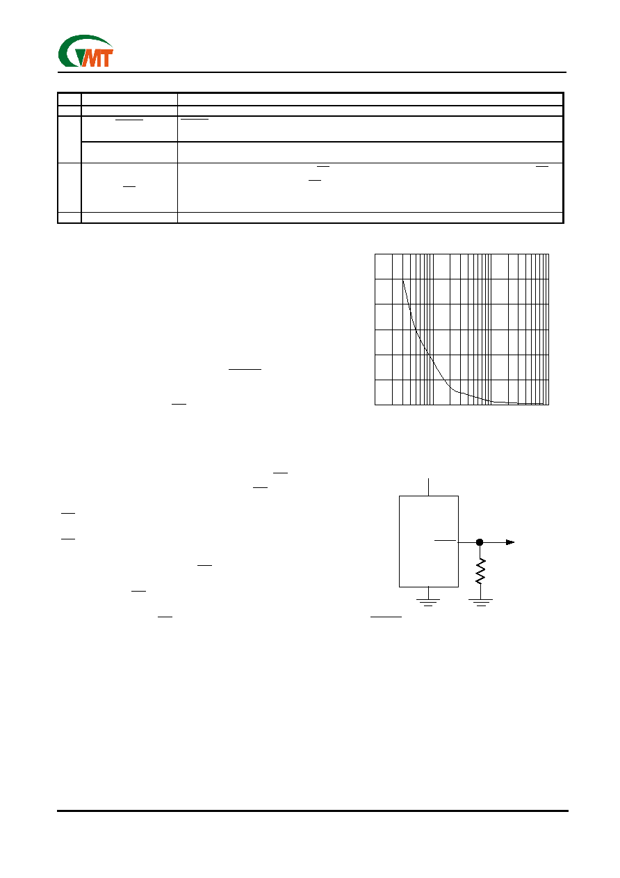
Figure 1.Maximum Transient Duration Without
Causing a Reset Pulse vs. Reset Com-
parator Overdrive
Figure2.
RESET
Valid to V
CC
= Ground Circuit
V
CC
RESET
GND
G692
R1
100k
V
CC
RESET
GND
G692
R1
100k
0
100
200
300
400
500
600
1
10
100
1000
Reset Comparator Overdrive, V
TH
-V
CC
(mV)
M
a
x
i
m
u
n
T
r
a
n
s
i
ent
Dur
a
t
i
on (
u
s)
Ver: 1.0
Sep 23, 2002
TEL: 886-3-5788833
http://www.gmt.com.tw
6
G692/G693
Global Mixed-mode Technology Inc.
Applications Information
Negative-Going V
CC
Transients
In addition to issuing a reset to the µP during power-up,
power-down, and brownout conditions, the
G693L/G692H/G692L are relatively immune to short-
duration negative-going V
CC
transients (glitches).
Figure1 shows typical transient duration vs. reset
comparator overdrive, for which the G693L/G692H/
G692L do not generate a reset pulse. The graph was
generated using a negative-going pulse applied to V
CC
,
starting 0.5V above the actual reset threshold and
ending below it by the magnitude indicated (reset
comparator overdrive). The graph indicates the maxi-
mum pulse width a negative-going V
CC
transient can
have without causing a reset pulse. As the magnitude
of the transient increases (goes farther below the reset
threshold), the maximum allowable pulse width de-
creases. Typically, for the G69_ _463 and G69_ _438,
a V
CC
transient that goes 100mV below the reset
threshold and lasts 15µs or less will not cause a reset
pulse. A 0.1µF bypass capacitor mounted as close as
possible to the V
CC
pin provides additional transient
immunity.
Ensuring a Valid Reset Output Down to V
CC
= 0
When V
CC
falls below 1V, the G692 RESET output no
longer sinks current--it becomes an open circuit.
Therefore, high-impedance CMOS logic inputs con-
nected to RESET can drift to undetermined voltages.
This presents no problem in most applications since
most µP and other circuitry is inoperative with
VCC
be-
low 1V. However, in applications where RESET must
be valid down to 0V, adding a pull-down resistor to
RESET causes any stray leakage currents to flow to
ground, holding RESET low (Figure 2). R1's value is
not critical; 100k
is large enough not to load RESET
and small enough to pull RESET to ground.
A 100k
pull-up resistor to
VCC
is also recommended
for the G693L if RESET is required to remain valid for
V
CC
< 1V.
Figure 3. Interfacing to µPs with Bidirectional Reset
I/O
Figure 4. G693L Open-Drain
RESET
Output Allows
Use with Multiple Supplies
Interfacing to µPs with Bidirectional Reset Pins
Since the RESET output on the G693L is open drain,
this device interfaces easily with µPs that have bidirec-
tional reset pins, such as the Motorola 68HC11. Con-
necting the µP supervisor's RESET output directly to
the microcontroller's (µC's) RESET pin with a single
pull-up resistor allows either device to assert reset
(Figure 3).
G693L Open-Drain
RESET
Output Allows Use with
Multiple Supplies
Generally, the pull-up connected to the G693L will
connect to the supply voltage that is being monitored at
the IC's V
CC
pin. However, some systems may use the
open-drain output to level-shift from the monitored sup-
ply to reset circuitry powered by some other supply
(Figure 4). Note that as the G693L's V
CC
decreases
below 1V, so does the IC's ability to sink current at
RESET . Also, with any pull-up, RESET will be pulled
high as V
CC
decays toward 0. The voltage where this
occurs depends on the pull-up resistor value and the
voltage to which it is connected.
Benefits of Highly Accurate Reset Threshold
Most µP supervisor ICs have reset threshold voltages
between 5% and 10% below the value of nominal sup-
ply voltages. This ensures a reset will not occur within
5% of the nominal supply, but will occur when the sup-
ply is 10% below nominal.
When using ICs rated at only the nominal supply ±5%,
this leaves a zone of uncertainty where the supply is
between 5% and 10% low, and where the reset may or
may not be asserted.
The G69_ _463/G69_ _308 use highly accurate circuitry
to ensure that reset is asserted close to the 5% limit,
and long before the supply has declined to 10% below
nominal.
RESET
INPUT
GND
5V SYSTEM
V
CC
RESET
GND
G693
V
CC
R
PULL-UP
+3.3V
+5.0
RESET
INPUT
GND
5V SYSTEM
V
CC
V
CC
R
PULL-UP
+3.3V
+5.0V
RESET
INPUT
GND
5V SYSTEM
V
CC
RESET
GND
G693
V
CC
R
PULL-UP
+3.3V
+5.0
RESET
INPUT
GND
5V SYSTEM
V
CC
V
CC
R
PULL-UP
+3.3V
+5.0V
RESET
INPUT
GND
µP
V
CC
RESET
GND
G693
V
CC
V
CC
MOTOROLA
68HCXX
R
PULL-UP
RESET
INPUT
GND
µP
V
CC
RESET
GND
G693
V
CC
V
CC
MOTOROLA
68HCXX
R
PULL-UP
Ver: 1.0
Sep 23, 2002
TEL: 886-3-5788833
http://www.gmt.com.tw
7
G692/G693
Global Mixed-mode Technology Inc.
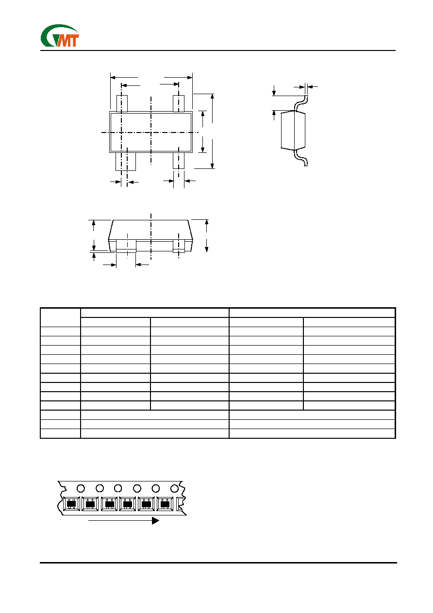
Package Information
SOT 143 Package
DIMENSION IN MILIMETERS
DIMENSION IN INCHS
SYMBOL
MIN. MAX. MIN.
MAX.
A 0.95
1.20
0.037
0.047
A1 0.05
0.10
0.002
0.004
A2 0.90
1.10
0.035
0.043
b 0.37
0.46
0.145
0.018
b1 0.76
0.89
0.030
0.035
C 0.10
0.18
0.004
0.007
D 2.80
3.04
0.110
0.120
E 1.20
1.40
0.047
0.055
E1 2.30
2.50
0.091
0.098
e1
1.92 BSC.
0.75 BSC.
e2
0.20 BSC.
0.078 BSC.
L
0.69 REF.
0.27 REF.
Package Orientation
GMT Inc. does not assume any responsibility for use of any circuitry described, no circuit patent licenses are implied and GMT Inc. reserves the right at any time without notice to change said circuitry and specifications.
E
D
E1
L
C
bx3
e2
e1
b1
A2
A1
A
E
D
E1
L
C
bx3
e2
e1
b1
A2
A1
A
b1
A2
A1
A
Feed Direction
SOT 143 Package Orientation
Feed Direction
SOT 143 Package Orientation